Lead process array etching method

An etching and array technology, applied in semiconductor/solid-state device manufacturing, nonlinear optics, semiconductor devices, etc., can solve the problems of low yield rate of Harima transistors, easily diffused silicon oxide film, low adhesion of insulating film, etc., to achieve guaranteed Yield, reduce production cost, improve the effect of yield

Inactive Publication Date: 2017-04-26
HKC CORP LTD +1
View PDF6 Cites 8 Cited by
  • Summary
  • Abstract
  • Description
  • Claims
  • Application Information

AI Technical Summary

Problems solved by technology

However, new metals also have some problems. For example, copper has low adhesion to glass substrates and insulating films, and is easy to diffuse into silicon oxide films. Therefore, titanium, molybdenum, etc. are usually used as the lower film metal to form metal multilayer film
[0004] After adopting the metal multilayer film, the manufacture of the Harima transistor has the problem of low yield rate, which brings troubles to those skilled in the art.

Method used


Image

  • Lead process array etching method
  • Lead process array etching method
  • Lead process array etching method

Examples


Embodiment Construction

[0043] In order to enable those skilled in the art to better understand the technical solutions in the present application, the technical solutions in the embodiments of the present application will be clearly and completely described below in conjunction with the drawings in the embodiments of the present application. Obviously, the described The embodiments are only some of the embodiments of the present application, but not all of them. Based on the embodiments in this application, all other embodiments obtained by persons of ordinary skill in the art without making creative efforts shall fall within the scope of protection of this application.

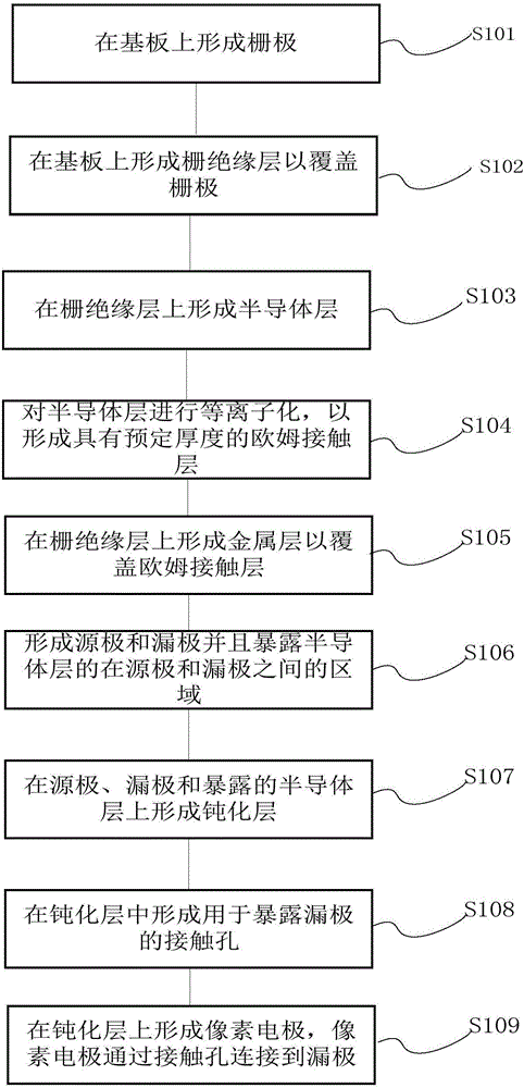
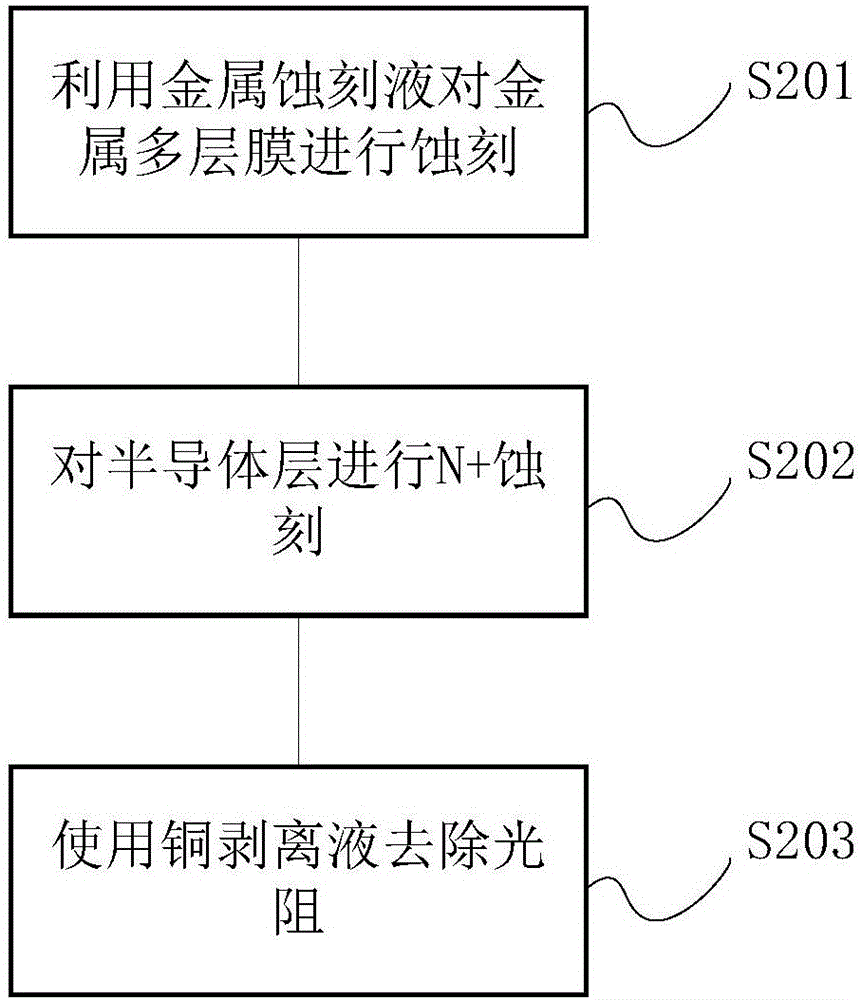
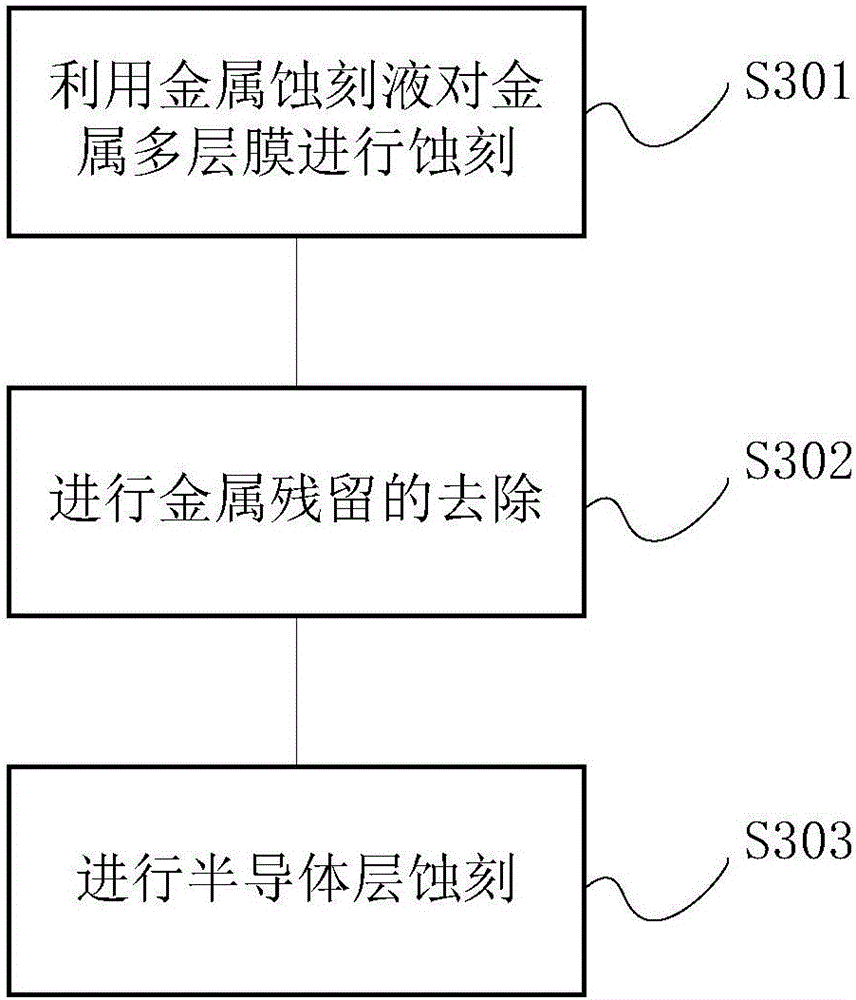
[0044] With the gradual development of TFT-LCDs towards ultra-large size, high drive frequency, and high resolution, high-quality wire manufacturing technology has become a necessary condition for the production of TFT-LCDs. How to effectively reduce the resistance of panel wires is very important. Therefore, replacing aluminum wir...


PUM


Abstract

The invention discloses a lead process array etching method comprising the following steps: using a metal etching liquid to etch metal multilayer films; removing metal residuals; etching a semiconductor layer. The method can prevent metal residuals so as to solve N+ residual problems, and thus improving product yield rate.

Description

technical field [0001] The invention relates to the field of display technology, in particular to a wire process array etching method. Background technique [0002] The microcircuits of semiconductor devices and liquid crystal display devices are formed on the substrate by conductive metal films such as aluminum, aluminum alloys, copper and copper alloys, or insulating films such as silicon dioxide films and silicon nitride films, and uniformly apply photolithography. Then through the patterned film, image after light irradiation, image the required pattern photoresist, use dry etching or wet etching, and display the pattern on the metal film or insulating film under the photoresist, It is completed by a series of photolithography processes such as stripping and removing unnecessary photoresist. [0003] Among them, the metal used for the source / drain, especially copper alloy, has low impedance and no environmental problems compared with the aluminum chrome wiring in the pr...

Claims


Application Information

Patent Timeline
Patent Type & Authority Applications(China)
IPC IPC(8): H01L21/02H01L21/3213H01L21/28H01L21/84H01L29/417
CPCH01L21/02068H01L21/32134H01L27/1259H01L29/41733H01L29/401H01L21/31133H01L27/124H01L21/30604H01L27/1288H01L21/0273G02F1/1368H01L29/45H01L29/66742
Inventor 陈猷仁
Owner HKC CORP LTD
Why Eureka
Try Eureka