Integrated silicon carbide Darlington transistor and manufacturing method thereof
A Darlington tube, integrated technology, applied in the field of microelectronics, can solve the problems of complex manufacturing process, small current handling capacity of the drive tube, and high cost
- Summary
- Abstract
- Description
- Claims
- Application Information
AI Technical Summary
Problems solved by technology
Method used
Image
Examples
Embodiment 1
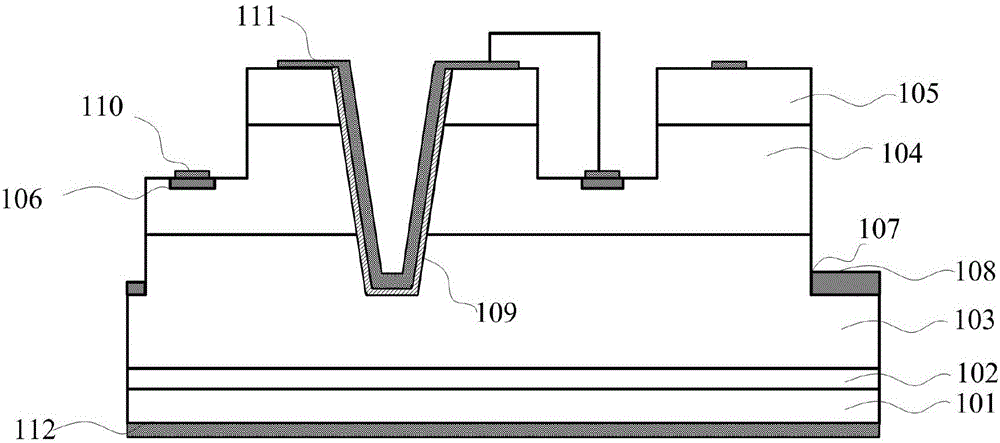
[0050] In the first step, the N+ buffer layer 102 is epitaxially grown on the N+ substrate 101 . Specifically, such as Figure 2A As shown, the N+ substrate 101 is firstly cleaned by RCA standard; and then epitaxially grown on the front surface of the N+ substrate 101 with a low-pressure hot-wall chemical vapor deposition method with a thickness of 3.5 μm and a nitrogen ion doping concentration of 8×10 17 cm -3 N+ buffer layer 102.
[0051] It should be noted that the growth conditions of the N+ buffer layer 102 are as follows: the temperature is 1600° C., the pressure is 100 mbar, the reaction gas includes silane and propane, the carrier gas is pure hydrogen, and the impurity source is liquid nitrogen.
[0052] It should be noted that the RCA standard cleaning method was first created by Kern and Puotinen in the RCA laboratory of N.J.Princeton in 1965, and thus got its name. RCA is a typical wet chemical cleaning method that is still the most commonly used. The cleaning me...
Embodiment 2
[0087] In step 1, an N+ buffer layer 102 is epitaxially grown on the N+ substrate 101 . Specifically, such as Figure 2A As shown, the N+ type silicon carbide substrate 10 is firstly cleaned by RCA standard; then, the epitaxial growth thickness is 5 μm and the nitrogen ion doping concentration is 1×10 18 cm -3 The buffer layer 102.
[0088] It should be noted that the growth conditions of the N+ buffer layer 102 are as follows: the temperature is 1600° C., the pressure is 100 mbar, the reaction gas includes silane and propane, the carrier gas is pure hydrogen, and the impurity source is liquid nitrogen.
[0089] Step 2, epitaxially growing the N- collector region 103 on the N+ buffer layer 102, specifically, as Figure 2B As shown, the buffer layer 102 is epitaxially grown on the buffer layer 102 with a thickness of 100 μm and a doping concentration of nitrogen ions of 2×10 14 cm -3 N-collector region 103 .
[0090] It should be noted that the growth process conditions o...
Embodiment 3
[0116] In step A, the N+ buffer layer 102 is epitaxially grown on the N+ substrate 101 . Specifically, such as Figure 2AAs shown, the N+ type silicon carbide substrate 10 is firstly cleaned by RCA standard; and then epitaxially grown on the front surface with a thickness of 6 μm and a nitrogen ion doping concentration of 5×10 18 cm -3 The buffer layer 102.
[0117] It should be noted that the growth conditions of the N+ buffer layer 102 are as follows: the temperature is 1600° C., the pressure is 100 mbar, the reaction gas includes silane and propane, the carrier gas is pure hydrogen, and the impurity source is liquid nitrogen.
[0118] Step B, epitaxially growing the N- collector region 103 on the N+ buffer layer 102, specifically, as Figure 2B As shown, the buffer layer 102 is epitaxially grown on the buffer layer 102 by the low-pressure hot-wall chemical vapor deposition method with a thickness of 105 μm and a nitrogen ion doping concentration of 6×10 14 cm -3 N-coll...
PUM
| Property | Measurement | Unit |
|---|---|---|
| width | aaaaa | aaaaa |
| thickness | aaaaa | aaaaa |
| thickness | aaaaa | aaaaa |
Abstract
Description
Claims
Application Information


