
Solar energy cell silicon chip etching water film solution and application thereof

A solar cell and water film technology, applied in the field of solar cells, can solve the problems of destroying the PN junction, aggravating the corrosion damage of the PN junction, and being unable to protect the PN junction very well, so as to achieve the effect of reducing damage

Active Publication Date: 2017-04-26
EGING PHOTOVOLTAIC TECHNOLOGY CO LTD
View PDF8 Cites 0 Cited by
  • Summary
  • Abstract
  • Description
  • Claims
  • Application Information

AI Technical Summary

Problems solved by technology

But the problem is: when etching or polishing with mixed acid, the high-concentration acid (such as HF, nitric acid, etc.) in the etching tank is easy to volatilize, and the volatilized acid will re-dissolve in the water film as the volatilization increases. Cause gas phase corrosion on the surface of the battery, destroying the PN junction on the surface; secondly, in order to remove the suede on the back of the silicon wafer to form a back polishing structure, a large amount of etching is required (generally refers to when the etching amount on the back of the silicon wafer is greater than or equal to 6 microns ), which further aggravates the corrosion damage to the PN junction, and the pure water film can no longer protect the front PN junction very well.

Method used


Image

  • Solar energy cell silicon chip etching water film solution and application thereof

Examples


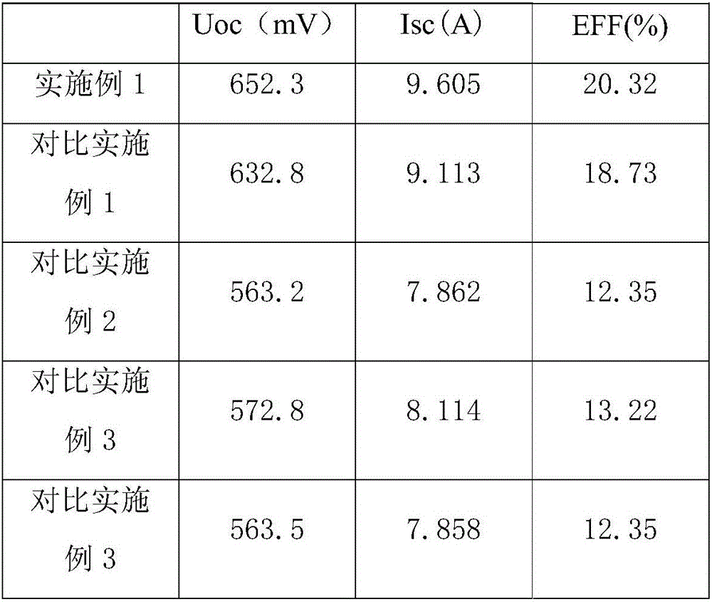
Embodiment 1

[0018] Preparation glucose content is 2.0g / L, bisfluorosulfonimide sodium content is the aqueous film solution of 0.25mol / L,

[0019] (1) Through the water film spray covering technology, the above-mentioned water film is sprayed on the diffusion surface formed by diffusion on the surface of the silicon wafer to form a flat water film protective layer, and the water film protective layer continues to exist until the silicon wafer Complete the etching step,

[0020] (2) Put the silicon wafer processed in step (1) into the etching tank, and the etching solution is commonly used HF / HNO 3 / H 2 SO 4 Mixed acid, in the etching tank, the silicon wafer is etched by floating on the etching solution,

[0021] The etch amount on the backside of the silicon wafer is 8 microns.


PUM


Abstract

The invention belongs to the solar energy cell technology field, and especially relates to a solar energy cell silicon chip etching water film solution and applications thereof; the solar energy cell silicon chip etching water film solution is formed by dispersing glucose and dual-fluorine sulfonyl imine salt into water; the water film solution can form a protection layer on the diffusing surface (front side) of the silicon chip, and enters an etching tank so as to etch PN nodes on the backside and edges, thus preventing acid, volatilized in the etching liquid, from re-dissolving in the water film, and reducing damages on PSG and PN nodes on the diffusing surface (front surface).

Description

technical field [0001] The invention belongs to the technical field of solar cells, and in particular relates to a water film solution for etching silicon wafers of solar cells and an application thereof. Background technique [0002] The general method of manufacturing silicon solar cells is as follows: first, the P-type or N-type silicon wafer with a clean surface undergoes a texturing process to form a textured structure; secondly, it is diffused on the surface of the silicon wafer to form an N+ or P+ emitter. Etch to remove the diffusion layer on the side and back of the silicon wafer; then form a layer of SiN film with anti-reflection function on the front surface; finally make metal electrodes on the front and back of the silicon wafer, and form a crystalline silicon solar cell through the sintering process. [0003] Among them, before wet etching, it is generally necessary to use a water film protection method. Before the silicon wafer enters the etching tank, a layer...

Claims


Application Information

Patent Timeline
Patent Type & Authority Applications(China)
IPC IPC(8): H01L31/0216H01L21/308H01L31/18
CPCH01L21/3081H01L21/3085H01L31/02167H01L31/1804H01L21/30604H01L31/068Y02E10/547
Inventor 孙铁囤张凯胜吴家宏
Owner EGING PHOTOVOLTAIC TECHNOLOGY CO LTD
Learn More