Wavelength division multiplexing light emission device based on array waveguide grating

An arrayed waveguide grating and emitting device technology, applied in the field of optical signal transmission, can solve the problems of complex optical path, difficult coupling and packaging, low coupling efficiency, etc., to simplify the optical path structure, increase the reliability and stability of the optical path, and reduce the packaging difficulty. Effect

Inactive Publication Date: 2017-05-10
众瑞速联(武汉)科技有限公司
View PDF4 Cites 9 Cited by
  • Summary
  • Abstract
  • Description
  • Claims
  • Application Information

AI Technical Summary

Problems solved by technology

[0003] The existing CWDM / Lan-WD wavelength division multiplexing optical transmitting devices all adopt the free-space optical path design scheme of the filter. In the filter group, multiple reflections are performed back and forth in the filter group to achieve wavelength multiplexing, and then after being collimated and focused by the second lens group, the combined light is emitted to realize light multiplexing; the existing filter The optical sheet realizes the spatial optical structure of wave division multiplexing, and the optical path is extremely complicated. First, a single optical filter unit must be accurately combined into a multi-channel optical filter group in a certain order, and then the optical input port, at least two lenses, etc. The coupling of the optical path of the optical group and the multi-channel filter group is extremely difficult; the solution must meet the smoothness of the four optical paths of the optical laser, output port, lens group, and multi-channel filter group at the same time.
Coupling efficiency is low, which runs counter to the development direction of low cost, miniaturization and integration of optical devices; based on the above reasons, there is an urgent need for technical improvement and improvement of existing optical devices to meet the needs of use

Method used


Image

  • Wavelength division multiplexing light emission device based on array waveguide grating

Examples


Embodiment Construction

[0014] The technical solution of this patent will be further described in detail below in conjunction with specific embodiments.

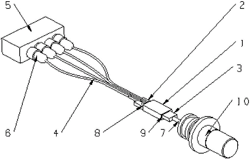
[0015] see figure 1 , a wavelength division multiplexing optical emission device based on an arrayed waveguide grating, comprising a planar optical waveguide integrated wavelength division multiplexing chip 1, a miniaturized package laser 5 and an optical fiber assembly; the optical fiber assembly includes a ceramic ferrule 6, a first coupling Port 8, second coupled port 9, first connecting fiber 4, second connecting fiber 7, four-channel fiber array 2 and single-channel fiber array 3; the four-channel fiber array 2 and single-channel fiber array 3 are used as light input The four-channel optical fiber array 2 and the single-channel optical fiber array 3 have the same channel number and channel spacing as the planar optical waveguide integrated wavelength division multiplexing chip 1.

[0016] The first connecting optical fiber 4 is an input optic...


PUM


Abstract

The invention discloses a wavelength division multiplexing light emission device based on an array waveguide grating. The wavelength division multiplexing light emission device comprises a miniaturized encapsulation laser device, wherein the miniaturized encapsulation laser device is in coupling connection with an input end surface of a planar optical waveguide integrated wavelength division multiplexing chip sequentially through a ceramic plug core, a first connecting fiber and a four-channel fiber array, and an output end of the planar optical waveguide integrated wavelength division multiplexing chip is connected with a light output port through a second connecting fiber; and one end of the first connecting fiber is fixed in the four-channel fiber array, the end surface of one end of the first connecting fiber is polished to form a first coupling port of a fiber assembly, one end of the second connecting fiber is fixed in a glass capillary, and the end surface of one end of the second connecting fiber is polished to form a second coupling port of the fiber assembly. The wavelength division multiplexing light emission device based on the array waveguide grating has the beneficial effects that the encapsulation difficulty is low, the encapsulation efficiency is high, and the reliability and stability of an optical path are high; the preparation cost is low, and the coupling efficiency is high; the producibility is extremely strong, and the repairability is high; and the wavelength division multiplexing light emission device can be widely applied to the wavelength multiplexing of light emitting devices.

Description

technical field [0001] The invention relates to the technical field of optical signal transmission, in particular to a wavelength division multiplexing optical transmitting device based on an arrayed waveguide grating. Background technique [0002] Optical devices are the cornerstone of optical communication modules, and the innovation of their technical solutions is the key to breaking through the bottleneck of optical module production; as data centers and high-performance computing applications place increasingly stringent requirements on the transmission rate and package size of optical components; for this The IEEE organization specially formulated the IEEE802.ba specification, which clarifies the 40G and 100G Ethernet transmission standards, uses CWDM / Lan-WDM wavelength division multiplexing technology to achieve 40G / 100G transmission rates, and conforms to specific package sizes. Devices are a huge challenge in the field of optical communications. [0003] The existi...

Claims


Application Information

Patent Timeline
Patent Type & Authority Applications(China)
IPC IPC(8): G02B6/42H04J14/02
CPCG02B6/421G02B6/4215G02B6/4296H04J14/0202
Inventor 杨明何伟炜印文健
Owner 众瑞速联(武汉)科技有限公司
Why Eureka
Try Eureka