Method of manufacturing micro LED chip with flip structure

A chip and flip-chip technology, applied in the field of fabrication of flip-chip microLED chips, can solve the problems of high cost, low yield, etc., and achieve the effects of high yield rate, high output efficiency, and good thermal conduction channels.

Inactive Publication Date: 2017-05-10
合肥彩虹蓝光科技有限公司
View PDF3 Cites 8 Cited by
  • Summary
  • Abstract
  • Description
  • Claims
  • Application Information

AI Technical Summary

Problems solved by technology

[0002] Micro LED is a replacement solution for LCD / OLED displays that have been popular in recent years. It has certain advantages in contrast and response speed, and its service life and energy consumption advantages are far superior to OLED / LCD displays. It is a display with relatively no shortcomings. Solutions; Apple, Sony, LG, Samsung and other major international manufacturers have all begun to focus on the development of Micro LED displays, but the current low yield rate and high cost limit their mass production

Method used


Image

  • Method of manufacturing micro LED chip with flip structure
  • Method of manufacturing micro LED chip with flip structure
  • Method of manufacturing micro LED chip with flip structure

Examples


Embodiment 1

[0023] A method for preparing a micro LED chip with a flip-chip structure, comprising the following steps:

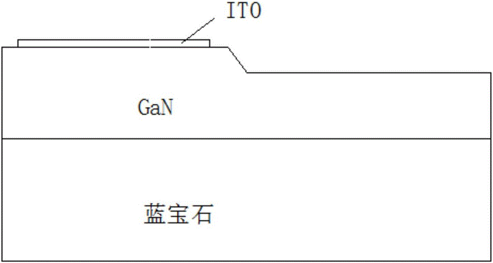
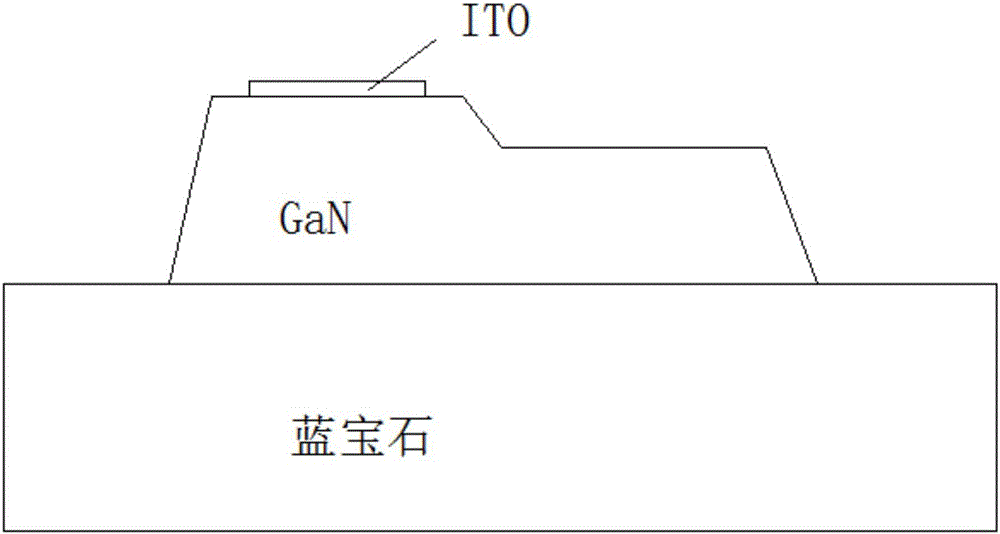
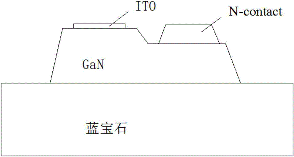
[0024] (1) Use a single-sided polished sapphire substrate to grow GaN epitaxy, and then grow an ITO film layer with a thickness of 20nm; then perform Mesa lithography and then Isolation lithography or first Isolation lithography and then Mesa lithography; single-sided polished sapphire substrate The thickness of the grown GaN epitaxy is 4 μm; the bare ITO film layer is etched after the Mesa pattern is etched, and the ICP etching is performed after the etching, and the etching depth is 1 μm to remove the photoresist; after Isolation photolithography ICP etching and removal of the photoresist, the surface Grown SiO 2 As a mask layer, the thickness is 1-2μm; after photolithography, use ICP dry etching to remove excess SiO 2 , etching gas optional SF 6 / CF 4 / CHF 3 ; use BCl afterwards 3 and Cl 2 Mixed gas etching GaN to Al 2 o 3 layer, remove photoresist, use HF / NH...

Embodiment 2

[0030] A method for preparing a micro LED chip with a flip-chip structure, comprising the following steps:

[0031] (1) Use a single-sided polished sapphire substrate to grow GaN epitaxy, and then grow an ITO film layer with a thickness of 100nm; then perform Mesa lithography and then Isolation lithography or first Isolation lithography and then Mesa lithography; single-sided polished sapphire substrate The thickness of GaN epitaxy growth is 8 μm; the exposed ITO film layer is etched after photolithography Mesa pattern, and ICP etching is performed after etching, and the etching depth is 2 μm to remove photoresist; after Isolation photolithography ICP etching and removal of photoresist, the surface Grown SiO 2 As a mask layer, the thickness is 2μm; use ICP dry etching after photolithography to remove excess SiO 2 , etching gas optional SF 6 / CF 4 / CHF 3 ; use BCl afterwards 3 and Cl 2 Mixed gas etching GaN to Al 2 o 3 layer, remove photoresist, use HF / NH 4 F mixed sol...

Embodiment 3

[0037] A method for preparing a micro LED chip with a flip-chip structure, comprising the following steps:

[0038](1) Use a single-sided polished sapphire substrate to grow GaN epitaxy, and then grow an ITO film layer with a thickness of 200nm; then perform Mesa lithography and then Isolation lithography or first Isolation lithography and then Mesa lithography; single-sided polished sapphire substrate The thickness of the grown GaN epitaxy is 10 μm; the exposed ITO film layer is etched after the Mesa pattern is etched, and the ICP etching is performed after the etching, and the etching depth is 3 μm to remove the photoresist; after Isolation photolithography ICP etching and removal of the photoresist, the surface Grown SiO 2 As a mask layer, the thickness is 1-2μm; after photolithography, use ICP dry etching to remove excess SiO 2 , etching gas optional SF 6 / CF 4 / CHF 3 ; use BCl afterwards 3 and Cl 2 Mixed gas etching GaN to Al 2 o 3 layer, remove photoresist, use H...


PUM


Abstract

The invention provides a method of manufacturing a micro LED chip with a flip structure. The method comprises the following steps: (1) single side polishing is selected to be carried out on a sapphire substrate to grow GaN epitaxy, an ITO film layer then grows, and Mesa photoetching first and then Isolation photoetching or Isolation photoetching first and then Mesa photoetching are carried out; (2) on a substrate after Mesa photoetching and Isolation photoetching are carried out in step (1), an N-contact pattern and a Passivation pattern are made in an N area; (3) photoetching is carried out on the substrate in the former step, a PN-contact pattern is made in a P area and the N area, vacuum evaporation is carried out on a metal electrode, the thickness is 1 to 3 mum, and a photoresist is removed; (4) an ITO film layer grows on the substrate in the former step, the thickness is 0.5 to 2 mum, photoetching is carried out, a specified pattern is etched, and the photoresist is removed; and (5) back grinding and polishing are carried out on the above substrate, the thickness range is 300 to 500 mum, and manufacturing is completed. The chip maximally utilizes the light emitting surface, and the chip with the same size can have higher brightness and lower energy consumption; and insulation protection is carried out on a possible electric leakage channel, and the electric leakage possibility generated to the chip due to a back process can be reduced.

Description

technical field [0001] The invention relates to the field of Micro LEDs, in particular to a method for preparing a flip-chip micro LED chip. Background technique [0002] Micro LED is a replacement solution for LCD / OLED displays that have been popular in recent years. It has certain advantages in contrast and response speed, and its service life and energy consumption advantages are far superior to OLED / LCD displays. It is a display with relatively no shortcomings. Solutions; Apple, Sony, LG, Samsung and other international manufacturers have all begun to focus on the development of Micro LED displays, but the current low yield rate and high cost limit their mass production. The polycrystalline transposition technology is a difficult point that needs to be overcome at the downstream display application side of the chip, and the design and manufacturing process of the chip itself also needs more optimization in terms of the size of the Micro LED. Contents of the invention ...

Claims


Application Information

Patent Timeline
Patent Type & Authority Applications(China)
IPC IPC(8): H01L33/00
CPCH01L33/007
Inventor 吴永军刘亚柱唐军吕振兴潘尧波
Owner 合肥彩虹蓝光科技有限公司
Why Eureka
Try Eureka