

Metal etching device and method
An etching device and metal technology, which is used in the manufacture/processing of electromagnetic devices to achieve the effect of improving the yield
- Summary
- Abstract
- Description
- Claims
- Application Information
AI Technical Summary
Problems solved by technology
Method used
Image

Examples
no. 1 example
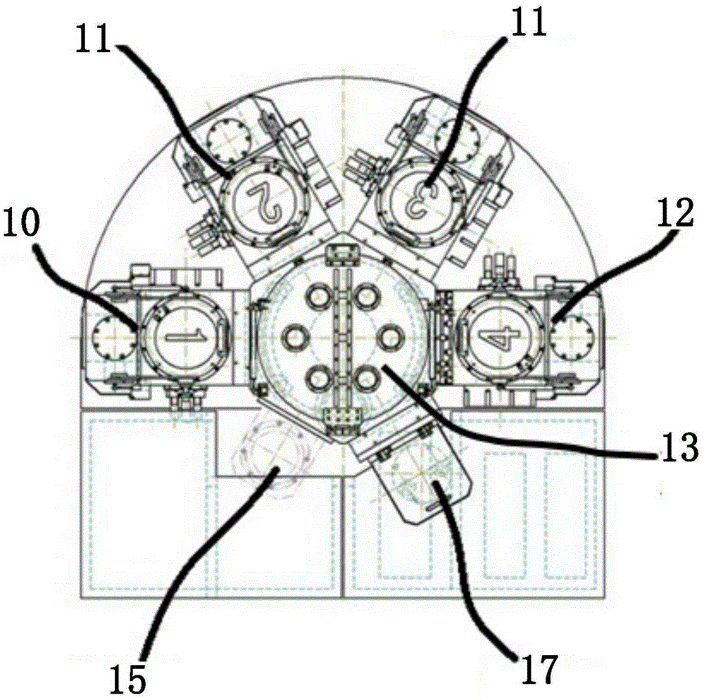
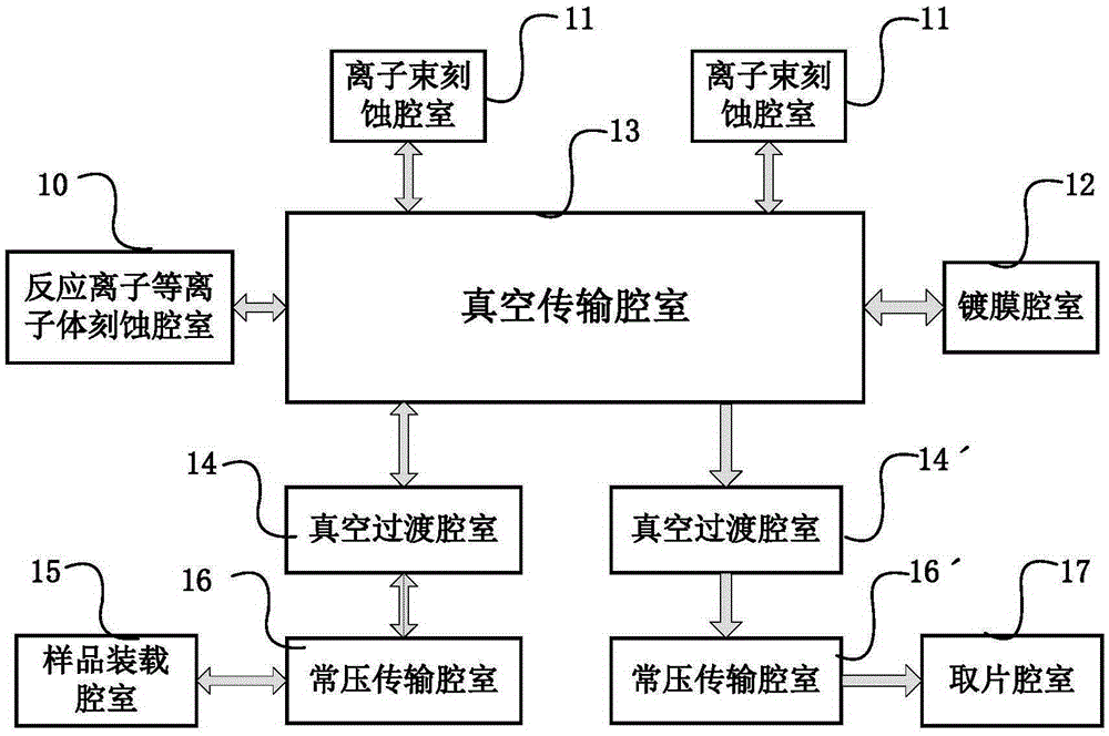
[0037] According to the first embodiment of the present invention, the metal etching device includes a reactive ion plasma etching chamber 10, an ion beam etching (IBE) chamber 11, a coating chamber 12, a vacuum transport chamber 13, a vacuum Transition chamber 14 ( figure 1 Not shown in ) and sample loading chamber 15. Wherein, the vacuum transition chamber 14 is respectively connected with the sample loading chamber 15 and the vacuum transmission chamber 13 in a communicable manner. The reactive ion plasma etching chamber 10 , the ion beam etching chamber 11 , and the coating chamber 12 are respectively connected to the vacuum transmission chamber 13 in a communicable manner. In addition, each of the above-mentioned chambers may also be multiple. figure 1 , figure 2 Two ion beam etching chambers 11 are shown in .
[0038] The metal etching device may also include an atmospheric pressure transmission chamber 16 ( figure 1 not shown in ), which are respectively connected...
no. 2 example
[0043] According to the second embodiment of the present invention, the metal etching device also includes a slice chamber 17, a vacuum transition chamber 14' ( figure 1 not shown in ), wherein, the taking-out chamber 17 is connected to the vacuum transition chamber 14' and the vacuum transfer chamber 13 in turn in a communicable manner. In addition, the metal etching device may also include a normal pressure transmission chamber 16' ( figure 1 not shown in ), which are respectively connected to the film taking chamber 17 and the vacuum transition chamber 14' in a communicable manner. Except for the above differences, the structures of other parts are the same as those of the first embodiment, and will not be described in detail again.
[0044] According to another aspect of the present invention, a metal etching method is provided. A detailed description will be given below in conjunction with the accompanying drawings. Figure 4 It is a flowchart showing the process flow ...
PUM
 Abstract
Description
Claims
Application Information