Preparation method for transistor ohmic contact electrode

A technology of ohmic contact electrodes and transistors, applied in semiconductor/solid-state device manufacturing, circuits, electrical components, etc., can solve the problems of reducing product performance and yield, reducing product reliability, and complex process, and improving yield and The effect of production efficiency, good surface quality and simple process

Inactive Publication Date: 2017-05-17
XIAMEN SANAN OPTOELECTRONICS TECH CO LTD
View PDF6 Cites 3 Cited by
  • Summary
  • Abstract
  • Description
  • Claims
  • Application Information

AI Technical Summary

Problems solved by technology

[0004] Regardless of the above-mentioned etching methods, the process is relatively complicated and requires very strict accuracy. A slight error will cause a series of problems, such as changes in current gain, reduced product reliability, and interface corrosion. On the one hand, it reduces the quality of the product. Performance and yield, on the other hand poor process controllability

Method used


Image

  • Preparation method for transistor ohmic contact electrode
  • Preparation method for transistor ohmic contact electrode
  • Preparation method for transistor ohmic contact electrode

Examples


Embodiment Construction

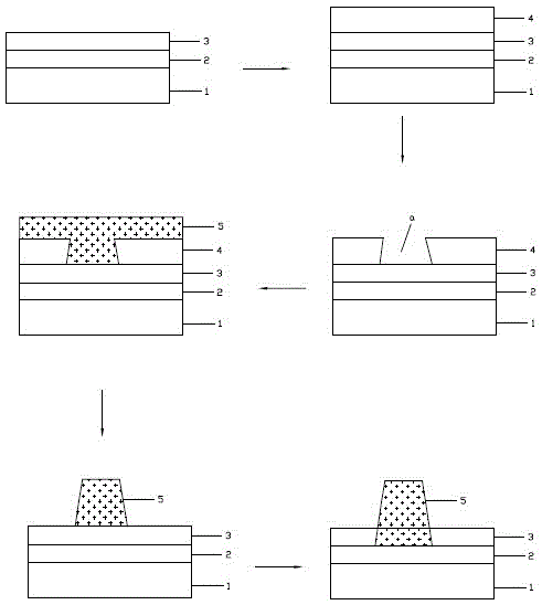
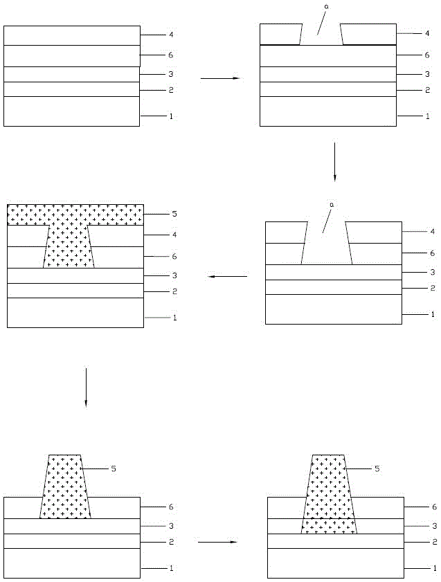
[0020] The present invention will be described in further detail below in conjunction with the accompanying drawings and embodiments. The drawings of the present invention are only schematic diagrams for easier understanding of the present invention, and their specific proportions can be adjusted according to design requirements. Those skilled in the art should understand that the upper and lower relationships of relative components in the figures described herein refer to the relative positions of the components, so all of them can be turned over to present the same components, which should all fall within the scope of the present specification. In addition, the number of elements and structures, the thickness of layers and the comparison of thicknesses between layers shown in the figure are only examples and are not limited thereto, and can be adjusted according to actual design requirements.

[0021] The following examples take the preparation method of the HBT base electro...


PUM

PropertyMeasurementUnit
thicknessaaaaaaaaaa
thicknessaaaaaaaaaa
thicknessaaaaaaaaaa

Abstract

The invention discloses a preparation method for a transistor ohmic contact electrode. The method comprises the steps of providing a semiconductor substrate containing a heavy doping P type GaAs layer and an InGaP layer; coating photoresist on the InGaP layer and forming at least one display area through exposure and development; depositing metal in the display area to form a metal layer; peeling off the photoresist; and at the temperature of 385-430 degrees centigrade, alloy 60-180 s, under the condition that the thickness of the P type GaAs layer is not smaller than 50 nm, the thickness of the InGaP layer is 30-50 nm, and the bottom of the metal layer at least comprises 20-50 nmPt, spreading the bottom of the metal layer to pass through the InGaP layer, thereby realizing the ohmic contact with the P type GaAs layer. The whole production process is simple, the time is saved, the controllability is greatly improved, and the yield of the products and the production efficiency are improved.

Description

technical field [0001] The invention relates to semiconductor technology, in particular to a method for preparing a transistor ohmic contact electrode. Background technique [0002] In the manufacturing process of transistors, the preparation of electrodes and the connection with corresponding semiconductor layers are an important link, which is a key factor affecting the performance and stability of integrated circuits. For example, a heterojunction bipolar transistor (HBT) usually includes a sequentially stacked collector layer, base layer, and emitter layer. In the prior art, when making the base electrode, it is necessary to use an etching process to remove even part of the emitter layer. The base layer is removed to expose the base layer by opening a window, and then metal is deposited on the exposed base layer to form a low-resistance, stable ohmic contact with the base layer. [0003] When removing part of the emitter semiconductor material, commonly used etching met...

Claims


Application Information

Patent Timeline
Patent Type & Authority Applications(China)
IPC IPC(8): H01L21/28H01L21/285
CPCH01L21/28506H01L21/28
Inventor 王江朱庆芳窦永铭许燕丽李斌魏鸿基
Owner XIAMEN SANAN OPTOELECTRONICS TECH CO LTD
Why Eureka
Try Eureka