
InP-based MOSHEMT structure and preparation method thereof

A technology of inxal1-xas and buffer layer, applied in the field of InP-based MOSHEMT structure and its preparation, can solve the problems of high electron mobility in conductive channel and two-dimensional electron gas concentration, restricting the development of InP-based HEMT devices, etc. Effects of electron mobility, reduction of MOS interface state density, and reduction of sheet resistance

Inactive Publication Date: 2017-05-24
INST OF MICROELECTRONICS CHINESE ACAD OF SCI
View PDF4 Cites 2 Cited by
  • Summary
  • Abstract
  • Description
  • Claims
  • Application Information

AI Technical Summary

Problems solved by technology

[0003] However, the channel two-dimensional electron gas concentration and electron mobility of traditional InP-based HEMTs cannot be achieved due to the influence of the material structure, so that the conductive channel electron mobility and two-dimensional electron gas concentration are both large, which limits the InP-based HEMT. The Development of Devices in Microwave Communication

Method used


Image

  • InP-based MOSHEMT structure and preparation method thereof
  • InP-based MOSHEMT structure and preparation method thereof

Examples


Embodiment Construction

[0035] "Up", "Down", "Inner" and "Outer" in the present invention are only used to indicate the relative positional relationship between each layer relative to the reference plane, and are not used to indicate the actual up-down and inner-outer relationship. The actual components can be Install in forward or reverse order according to specific needs. Also, "over" and "under" represent contact and non-contact with the target layer.

[0036] In order to make the object, technical solution and advantages of the present invention clearer, the present invention will be further described in detail below in conjunction with specific embodiments and with reference to the accompanying drawings.

[0037] It should be noted that implementations not shown or described in the accompanying drawings are forms known to those of ordinary skill in the art. Additionally, while illustrations of parameters including particular values ​​may be provided herein, it should be understood that the para...


PUM


Abstract

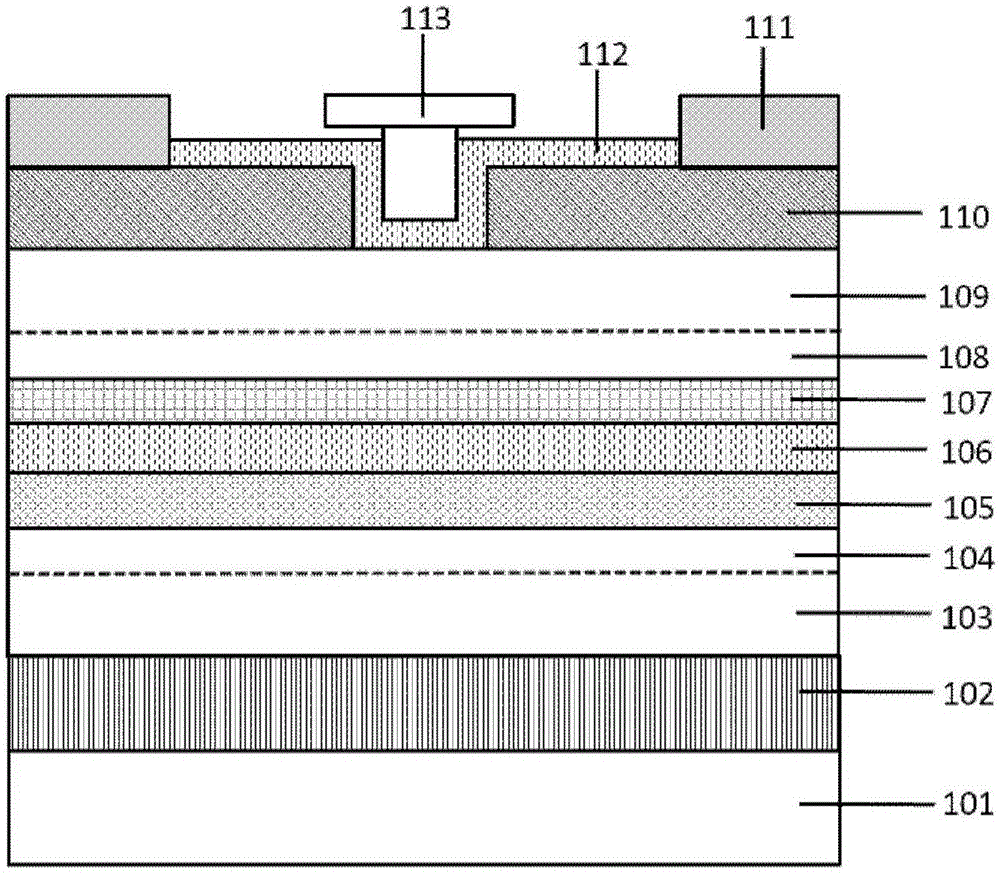
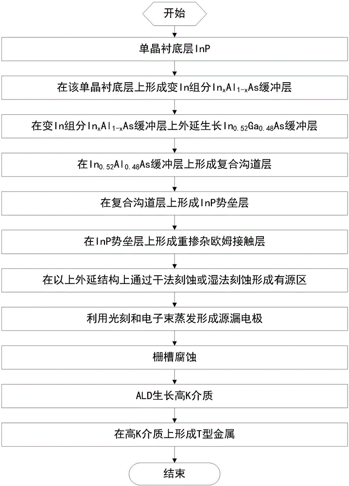
The present invention discloses an InP-based MOSHEMT structure and a preparation method thereof. The structure comprises from up to down in order: a single crystal substrate (101); a variable In component InxAl(1-x)As buffer layer (102) formed on the upper surface of the single crystal substrate; an In0.52Al0.48As buffer layer (103); a planar doping layer (104) formed in the buffer layer; an In0.7Ga0.3As channel layer (105); an In0.6Ga0.4As channel layer (106); an In0.5Ga0.5As channel layer (107); an InP barrier layer (108); and a planar doping layer (109) formed in the barrier layer. The InP-based MOSHEMT structure and the preparation method thereof employ a component gradual changing buffer layer to reduce the lattice mismatch between III-V semiconductors so as to reduce the defects caused by dislocation. The device structure reduces the MOS interface state density and employs a high In component In0.7 Ga0.3As / In0.6Ga0.4As / In0.5Ga0.5As composite channel design to fully improve the concentration and the electronic mobility of the two two-dimensional electron gas and reduce the square resistance of the channel.

Description

technical field [0001] The invention relates to the technical field of semiconductor devices, in particular to an InP-based MOSHEMT structure and a preparation method thereof. Background technique [0002] At present, the mainstream of the semiconductor industry is silicon technology. With the development of the smallest size of semiconductor technology to the nanometer scale, silicon integrated circuit technology is increasingly approaching its theoretical and technical double limit. Compared with silicon materials, III-V semiconductor materials have higher electron mobility (6-60 times) and have more excellent electron transport properties under low electric field and strong field. Therefore, III-V semiconductor materials Materials will be an inevitable choice for a new generation of ultra-high frequency and low power integrated electronic systems. [0003] However, the channel two-dimensional electron gas concentration and electron mobility of traditional InP-based HEMTs...

Claims


Application Information

Patent Timeline
Patent Type & Authority Applications(China)
IPC IPC(8): H01L29/778H01L29/10H01L29/207H01L29/36H01L21/335
CPCH01L29/7786H01L29/1029H01L29/207H01L29/365H01L29/66462
Inventor 王盛凯刘洪刚孙兵李跃常虎东王博
Owner INST OF MICROELECTRONICS CHINESE ACAD OF SCI
Learn More