Composite transparent conductive film and preparation method thereof

A technology of transparent conductive film and transparent conductive layer, which is applied in ion implantation plating, metal material coating process, coating, etc., can solve the problems of high cost of transparent conductive film, lower conductivity than ITO, and inability to pass environmental tests, etc. Achieve the effect of excellent light transmission, reduce the complexity of operation, and stabilize the environment test

Inactive Publication Date: 2017-05-31
SHAANXI NORMAL UNIV
View PDF6 Cites 3 Cited by
  • Summary
  • Abstract
  • Description
  • Claims
  • Application Information

AI Technical Summary

Problems solved by technology

The existing transparent conductive films are all prepared by pure ITO or AZO, but the cost of pure ITO transparent conductive films is relatively high, and sometimes they cannot pass the environmental test, and sometimes spots appear in high temperature and high humidity environmen...

Method used


Image

  • Composite transparent conductive film and preparation method thereof
  • Composite transparent conductive film and preparation method thereof
  • Composite transparent conductive film and preparation method thereof

Examples


Embodiment 1

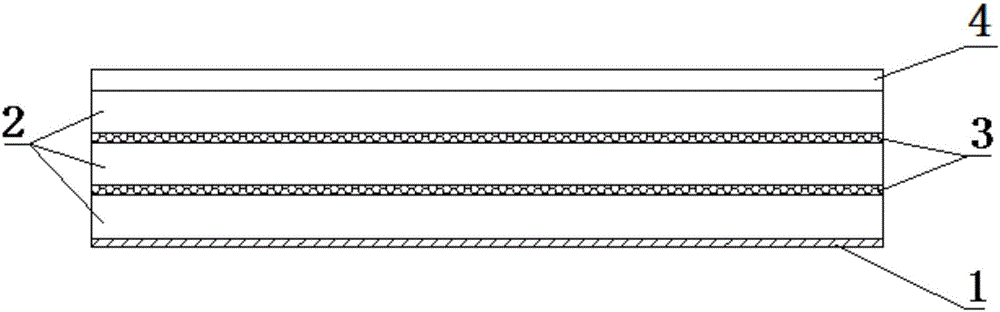
[0046] Step 1, using H 2 -Ar mixed gas plasma method to treat the substrate surface and activate the surface;

[0047] Step 2, depositing a layer of prefabricated titanium nano-metal layer on the flexible substrate PET, the conditions are as follows:

[0048]

[0049] Step 3, use sputtering equipment to sputter doped zinc oxide film on the prefabricated layer, and the sputtering conditions are as follows:

[0050]

[0051] The average light transmittance in the visible light region is >70%, and the resistivity is >10 -3 ohm cm

[0052] Step 4, sputtering the ITO film on the existing doped zinc oxide film with a sputtering device, the sputtering conditions are as follows:

[0053]

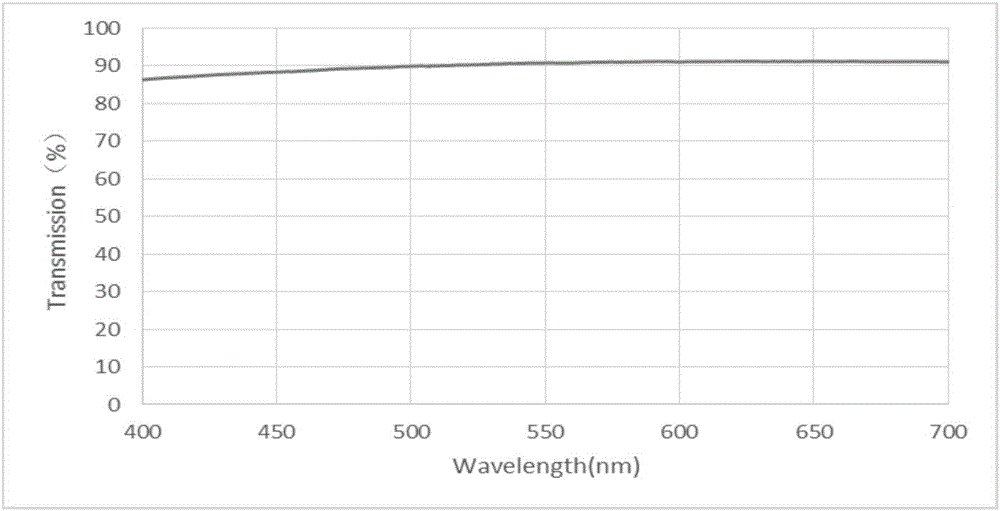
[0054] Result: light transmittance 83%, resistivity 6×10 -4 Ω. cm.

Embodiment 2

[0056] Step 1, using H 2 -Ar mixed gas plasma method to treat the substrate surface and activate the surface;

[0057] Step 2, depositing a layer of prefabricated titanium nano-metal layer on the flexible substrate PET, the conditions are as follows:

[0058]

[0059] Step 3, use sputtering equipment to sputter doped zinc oxide film on the prefabricated layer, and the sputtering conditions are as follows:

[0060]

[0061] The average light transmittance in the visible light region is >70%, and the resistivity is >10 -3 ohm cm

[0062] Step 4, using sputtering equipment to sputter silver nanoparticles on the existing doped zinc oxide film, the sputtering conditions are as follows:

[0063] Working pressure (Pa) temperature(℃) Power (W) Particle size (nm) 1.4×10 ‐4

200 120 200

[0064] Step 5, use sputtering equipment to sputter the ITO film on the existing silver nanoparticles, and the sputtering conditions are as follows:

[0065]

...

Embodiment 4

[0069] Step 1, using H 2 -Ar mixed gas plasma method to treat the substrate surface and activate the surface;

[0070] Step 2, depositing a layer of prefabricated titanium nano-metal layer on the flexible substrate PET, the conditions are as follows:

[0071]

[0072] Step 3, use sputtering equipment to sputter doped zinc oxide film on the prefabricated layer, and the sputtering conditions are as follows:

[0073]

[0074] The average light transmittance in the visible light region is >70%, and the resistivity is >10 -3 ohm cm

[0075] Step 4, using sputtering equipment to sputter a heavily doped indium oxide transparent conductive layer on the existing doped zinc oxide film, the sputtering conditions are as follows:

[0076]

[0077] Step 5, using a sputtering device to sputter an ITO layer on the existing heavily doped indium oxide transparent conductive layer, the sputtering conditions are as follows:

[0078]

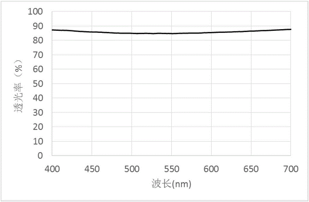
[0079] The average light transmittance in the ...


PUM

PropertyMeasurementUnit
Resistivityaaaaaaaaaa

Abstract

The invention relates to a composite transparent conductive film and a preparation method thereof. The composite transparent conductive film comprises a substrate, at least one layer of zinc oxide-doped transparent conductive film deposited on the substrate, an ITO layer deposited on the topmost layer, and at least one layer of heavily-doped transparent conductive film or nano-particles deposited on the composite transparent conductive film. The preparation method of the composite transparent conductive film includes the following steps of (1), depositing the first zinc oxide-doped transparent conductive film layer on the pretreated substrate; (2), preparing a layer of heavily-doped transparent conductive film with the thickness no more than 2000 nm, or nano-particles with the particle size no more than 2000 nm; (3), depositing a layer of zinc oxide-doped transparent conductive film or nano-particles on the heavily-doped transparent conductive film; and (4), repeating the step (2) and/or the step (3) till reaching the required technical parameters, depositing the ITO layer on the topmost layer, and obtaining the composite transparent conductive film finally.

Description

technical field [0001] The invention relates to a conductive thin film material, in particular to a composite transparent conductive thin film and a preparation method thereof. Background technique [0002] Transparent conductive film is a functional film with good conductivity and good transmittance in the visible light range. It mainly includes metal film system, oxide film system, other compound film system, polymer film system and composite film system. Wait. At present, the most widely studied and applied are the metal film system and the oxide film system. Transparent conductive films are mainly used as window materials for optoelectronic devices (such as LEDs, thin-film solar cells, etc.). Common transparent conductive films are ITO (tin-doped indium trioxide), AZO (aluminum-doped zinc oxide) and other transparent conductive films that not only require good electrical conductivity, but also have excellent visible light transmittance. The existing transparent conduc...

Claims


Application Information

Patent Timeline
IPC IPC(8): C23C14/08C23C14/20C23C14/18
CPCC23C14/086C23C14/185C23C14/205
Inventor 刘生忠朱学杰冯江山肖锋伟
Owner SHAANXI NORMAL UNIV
Why Eureka
Try Eureka