LED epitaxial wafer grown on glass substrate and preparation method thereof
An LED epitaxial wafer and glass substrate technology, applied in semiconductor devices, electrical components, circuits, etc., can solve the problems of expensive sapphire and SiC substrates, high prices, and high LED manufacturing costs, and achieve easy acquisition, easy removal, The effect of reducing production costs
- Summary
- Abstract
- Description
- Claims
- Application Information
AI Technical Summary
Problems solved by technology
Method used
Image
Examples
Embodiment 1
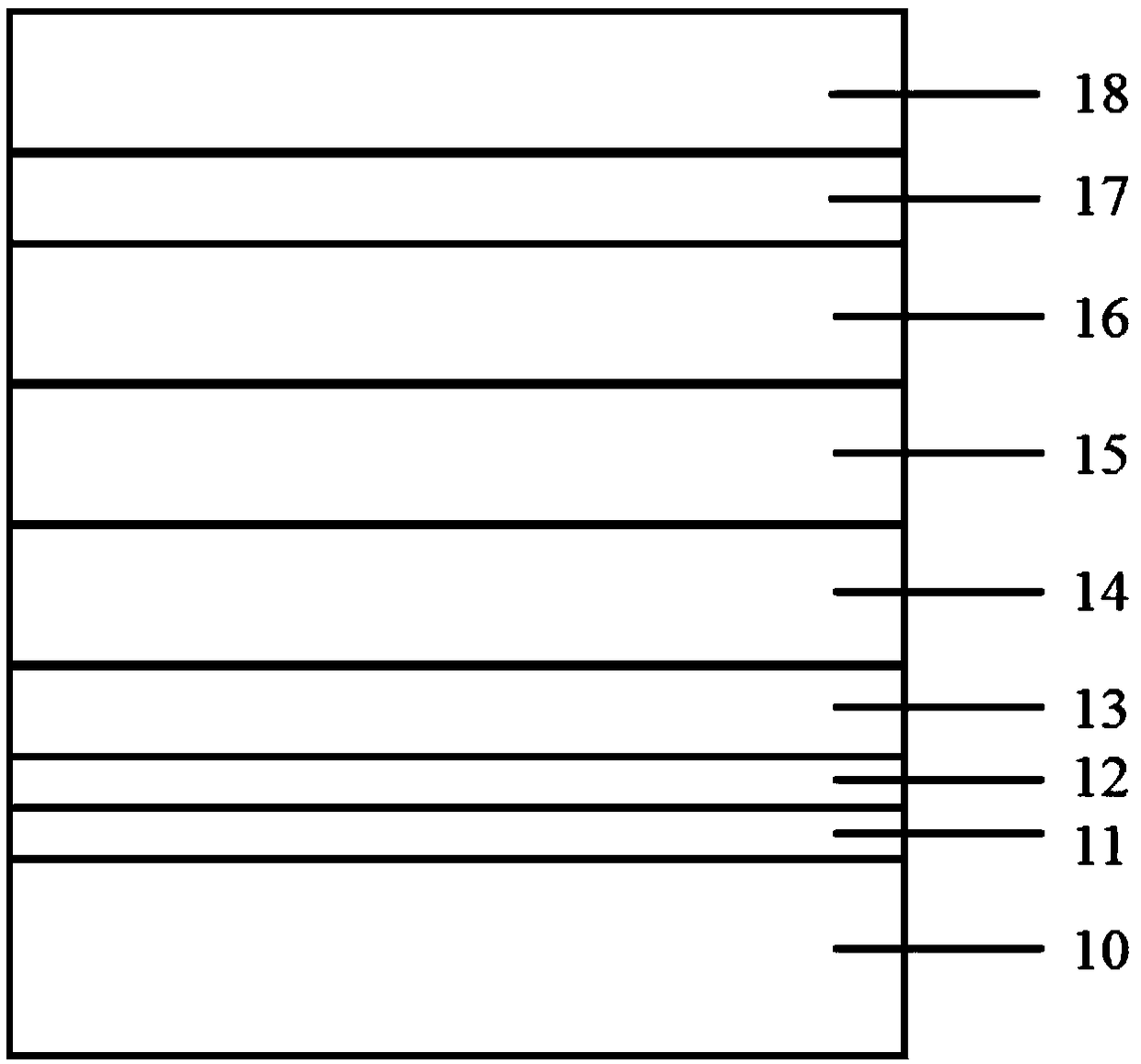
[0039] Such as figure 1 As shown, the LED epitaxial wafer grown on the glass substrate prepared in this embodiment includes the aluminum metal layer 11 grown on the glass substrate 10, the silver metal layer 12 grown on the aluminum metal layer 11, and the silver metal layer 12 grown on the silver metal layer. AlN buffer layer 13 on layer 12, GaN buffer layer 14 grown on AlN buffer layer 13, undoped GaN layer 15 grown on GaN buffer layer 14, n-type doped GaN layer grown on undoped GaN layer 15 Doped GaN thin film 16, InGaN / GaN quantum well 17 grown on n-type doped GaN thin film 16, p-type doped GaN thin film 18 grown on InGaN / GaN quantum well 17.
[0040] The preparation method of the LED epitaxial wafer grown on the glass substrate of the present embodiment comprises the following steps:
[0041] (1) Selection of substrate: use ordinary glass substrate;
[0042] (2) Substrate surface polishing and cleaning treatment;
[0043] The surface polishing of the substrate is speci...
Embodiment 2
[0057] The preparation method of the LED epitaxial wafer grown on the glass substrate of the present embodiment comprises the following steps:
[0058] (1) Selection of substrate: use ordinary glass substrate;
[0059] (2) Substrate surface polishing and cleaning treatment;
[0060] The surface polishing of the substrate is specifically:
[0061] First, the surface of the glass substrate is polished with diamond slurry, and the surface of the substrate is observed with an optical microscope until there are no scratches, and then the chemical mechanical polishing method is used for polishing;
[0062] The cleaning is specifically:
[0063] Put the glass substrate into deionized water and ultrasonically clean it at room temperature for 5 minutes to remove the dirt particles on the surface of the glass substrate, then wash it with acetone and ethanol in sequence to remove the surface organic matter, and dry it with high-purity dry nitrogen;
[0064] (3) Growth of the aluminum ...
PUM
| Property | Measurement | Unit |
|---|---|---|
| thickness | aaaaa | aaaaa |
| thickness | aaaaa | aaaaa |
| thickness | aaaaa | aaaaa |
Abstract
Description
Claims
Application Information

