Semiconductor laser unit with pectinate current distribution and manufacturing method thereof

A current distribution and semiconductor technology, which is applied in the field of semiconductor lasers with comb-shaped current distribution and its production, can solve the problems of device performance impact, difficult production process, etc., meet the requirements of lower production process, strong anti-external feedback ability, high Effect of side mode suppression ratio

Pending Publication Date: 2017-05-31
FUJIAN INST OF RES ON THE STRUCTURE OF MATTER CHINESE ACAD OF SCI
View PDF6 Cites 1 Cited by
  • Summary
  • Abstract
  • Description
  • Claims
  • Application Information

AI Technical Summary

Problems solved by technology

[0004] To sum up, there are certain difficulties in the manufacturing process of semiconductor lasers containing Bragg gratings. The refractive index coupling type is easy to carry out secondary epitaxy after the grating is prepared; the manufacturing of the gain coupling type involves the processing of the active region. It has a great impact on the performance of the device; the manufacturing process of DBR-LD is more difficult than that of DFB-LD

Method used


Image

  • Semiconductor laser unit with pectinate current distribution and manufacturing method thereof
  • Semiconductor laser unit with pectinate current distribution and manufacturing method thereof
  • Semiconductor laser unit with pectinate current distribution and manufacturing method thereof

Examples


Embodiment 1

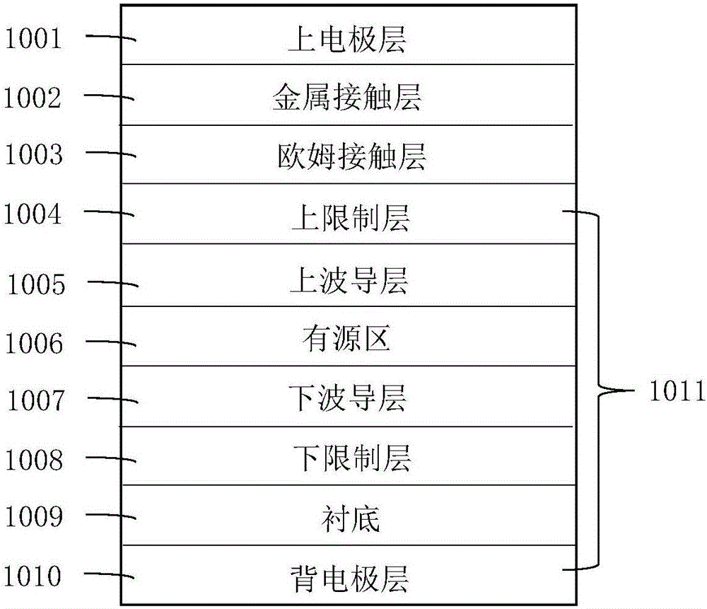
[0047] Such as figure 1 and image 3 As shown, the structure of the semiconductor laser is specifically: on the InP substrate 1009, there are successively a 1 μm InP lower confinement layer 1008, a 100nm InGaAsP lower waveguide layer 1007, a multi-quantum well active region 1006, a 100nm InGaAsP upper waveguide layer 1005, and a 300nm InP upper confinement layer. layer 1004, 200nm InGaAs ohmic contact layer 1003, Ti-Pt-Au metal contact layer 1002, upper electrode layer 1001, and the back electrode layer 1010 under the substrate 1009.

[0048] Among them, the multi-quantum well active region 1006 uses InGaAsP as the quantum well, AlGaInAs or InGaAsP as the potential barrier, the number of quantum well layers is 3-10 layers, the thickness of the quantum well layer is 5-8nm, and the thickness of the barrier layer is 5-10nm. It is 1.2%, and the central lasing wavelength is in the range of 1.2um-1.7um (specific parameters vary according to different designs).

[0049] The metal c...

Embodiment 2

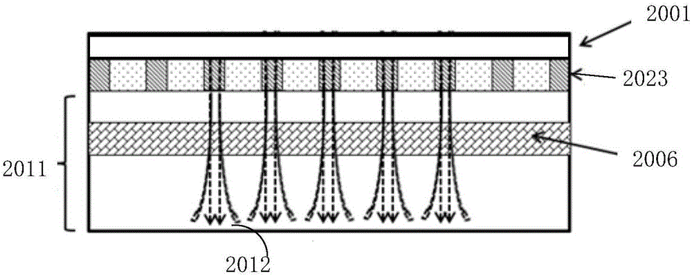
[0060] This example Figure 4 As shown, the difference between it and Embodiment 1 is that the resistance of the metal contact layer 3002 in Embodiment 1 is a comb-shaped distribution structure, and the ohmic contact layer 4003 on the general structure 4011 in this embodiment includes a high resistance region 4027 and a low resistance In the region 4026, the resistance is distributed regularly in a comb shape, and the metal contact layer 4002 has a uniform distribution of resistance. Alternatively, the high resistance region 4027 may also be an oxide insulating region.

[0061] The manufacturing process of the semiconductor laser in this embodiment is,

[0062] 1) The MOCVD growth epitaxial structure includes: a lower confinement layer, a lower waveguide layer, an active region, an upper waveguide layer, an upper confinement layer, and an ohmic contact layer 4003;

[0063] 2) After electron beam exposure (or holographic lithography), diffusion or ion beam bombardment prepare...

Embodiment 3

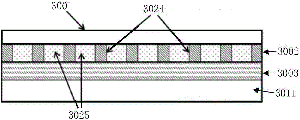
[0071] This example Figure 5 As shown, the difference between this embodiment and Embodiment 1 is that the comb structure in Embodiment 1 covers the entire metal contact layer 3002, and a part of the metal contact layer 5002 in this embodiment is a comb-shaped metal contact region 5024 and a comb-shaped The comb-like metal contact region 5023 formed by the oxidation insulating region 5025 is a uniform metal contact region 5029 . The comb-shaped metal contact region 5023 is located at one end of the uniform metal contact region 5029 (such as Figure 5 shown), or the comb-shaped metal contact region 5023 is located at both ends of the uniform metal contact region 5029 (not shown). Reference numeral 5011 denotes a general structure.

[0072] The manufacturing process of the semiconductor laser in this embodiment is:

[0073] 1) An epitaxial structure grown by MOCVD, the epitaxial structure comprising: a lower confinement layer, a lower waveguide layer, an active region, an up...


PUM


Abstract

The invention relates to a semiconductor laser unit with pectinate current distribution and a manufacturing method thereof. The semiconductor laser unit comprises a substrate, a metal contact layer and an ohmic contact layer; a resistive pectinate distribution structure is adopted for the substrate or the metal contact layer or the ohmic contact layer, or the resistive pectinate distribution structure is adopted for the substrate and the metal contact layer, or the resistive pectinate distribution structure is adopted for the substrate and the ohmic contact layer, or the resistive pectinate distribution structure is adopted for the metal contact layer and the ohmic contact layer, or the resistive pectinate distribution structure is adopted for the substrate, the metal contact layer and the ohmic contact layer. The semiconductor laser unit with a gain-refractive index combined coupling grating is realized by manufacturing a metal contact region or an ohmic contact region of the laser unit to be of the resistive pectinate distribution structure. A secondary epitaxy technology may not be involved, so that the manufacturing difficulty of the device is lowered, and meanwhile many advantages of a gain coupling grating semiconductor laser unit are reserved.

Description

technical field [0001] The invention relates to a semiconductor device, in particular to a semiconductor laser with comb-like current distribution and a manufacturing method thereof. Background technique [0002] Distributed Feedback (DFB) semiconductor laser (DFB-LD) and distributed Bragg reflector (Distributed Bragg Reflector, DBR) semiconductor laser (DBR-LD) both realize optical feedback by including Bragg gratings. The difference between the two lies in the position of the grating and the active area. In 1972, H. Kogelnik and C.V. Shank pointed out in the theoretical analysis that there are two basic feedback methods in DFB-LD, one is the Bragg reflection caused by the periodic change of the refractive index, That is, the refractive index coupling type (Index-Coupling), and the other is the distributed feedback caused by the periodic change of the gain, that is, the gain coupling (Gain-Coupling). Compared with F-P cavity lasers, which rely on two reflective end faces ...

Claims


Application Information

Patent Timeline
Patent Type & Authority Applications(China)
IPC IPC(8): H01S5/02
CPCH01S5/02
Inventor 林琦林中晞陈景源陈阳华苏辉薛正群王凌华林乐
Owner FUJIAN INST OF RES ON THE STRUCTURE OF MATTER CHINESE ACAD OF SCI
Why Eureka
Try Eureka