Multistage amplifier

A multi-stage amplifier and MOS tube technology, applied in the direction of amplifiers, differential amplifiers, DC-coupled DC amplifiers, etc., can solve the problems of amplifier gain bandwidth reduction, amplifier power supply voltage reduction, large circuit scale, etc., and achieve the effect of improving gain

Active Publication Date: 2017-05-31
SHANGHAI HUAHONG GRACE SEMICON MFG CORP
View PDF7 Cites 3 Cited by
  • Summary
  • Abstract
  • Description
  • Claims
  • Application Information

AI Technical Summary

Problems solved by technology

However, as the process size continues to shrink, the supply voltage of the amplifier continues to decrease, which reduces the gain and output swing of the amplifier, which in turn reduces the gain bandwid...

Method used


Image

  • Multistage amplifier
  • Multistage amplifier
  • Multistage amplifier

Examples


Embodiment Construction

[0033] As mentioned in the background section, in the prior art, the number of amplifier stages is usually increased to solve the technical problem of low gain and unity gain bandwidth of the amplifier.

[0034] Specifically, the inventor of the present application analyzed a multi-stage amplifier in the prior art.

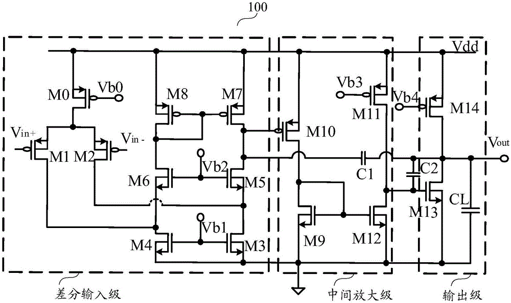
[0035] Such as figure 1 As shown, the multi-stage amplifier 100 may include a differential input stage, at least one intermediate amplification stage, and an output stage. The multi-stage amplifier 100 is only taken as an example including a single intermediate amplification stage.

[0036] In the differential input stage, the voltage-controlled current source composed of MOS transistor M0 is suitable for providing bias current to the outside to ensure the normal operation of the differential input stage; MOS transistors M1, M2, M3, and M4 constitute the folded differential input Cascode structure, MOS transistors M5 to M8 are differential input stage loads, whe...


PUM


Abstract

The invention discloses a multistage amplifier which comprises a differential input stage, at least one intermediate amplification stage and an output stage. The differential input stage, the intermediate amplification stages and the output stage are sequentially in cascade connection with one another; the differential input stage comprises a first MOS (metal oxide semiconductor) transistor, a second MOS transistors, a third MOS transistor, a fourth MOS transistor, a first current mirror circuit, a second current mirror circuit, a first bias circuit and a first load circuit, source electrodes and grid electrodes of the first MOS transistor and the second MOS transistor are coupled with one another, and first voltages can be received by the grid electrodes of the first MOS transistor and the second MOS transistor; source electrodes and grid electrodes of the third MOS transistor and the fourth MOS transistor are coupled with one another, second voltages can be received by the grid electrodes of the third MOS transistor and the fourth MOS transistor, the source electrodes of the third MOS transistor and the second MOS transistor are coupled with each other, and first bias currents can be received by the source electrodes of the third MOS transistor and the second MOS transistor; a common grid electrode of the first current mirror circuit is coupled with a drain electrode of the third MOS transistor, and a first drain electrode of the first current mirror circuit is coupled with a drain electrode of the first MOS transistor; a common grid electrode of the second current mirror circuit is coupled with a drain electrode of the second MOS transistor, and a first drain electrode of the second current mirror circuit is coupled with a drain electrode of the fourth MOS transistor; the first bias circuit is suitable for providing bias circuits for the first current mirror circuit and the second current mirror circuit; the first load circuit is suitable for providing load for the differential input stage. According to the scheme, the multistage amplifier has the advantages of high gain and wide unity gain bandwidth.

Description

technical field [0001] The invention relates to the field of analog circuit design, in particular to a multi-stage amplifier. Background technique [0002] Operational amplifier (hereinafter referred to as amplifier) ​​is a basic device of analog integrated circuit. The application requirements for amplifiers are generally high gain, high bandwidth, and high slew rate. [0003] For example, a typical multi-stage amplifier in the prior art may include a differential input stage, at least one intermediate amplifier stage, and an output stage; wherein, optionally, the differential input stage may adopt a cascode structure, and may include four MOS The current mirror load contained in it can convert the differential signal into a single-ended signal and output it; the intermediate amplifier stage can be a common source structure, and further amplify the single-ended signal output by the differential input stage; the The output stage is adapted to improve the load carrying capa...

Claims


Application Information

Patent Timeline
IPC IPC(8): H03F3/45
CPCH03F3/45H03F3/45273H03F2200/366
Inventor 戴若凡
Owner SHANGHAI HUAHONG GRACE SEMICON MFG CORP
Why Eureka
Try Eureka