

Etching solution composition, array substrate for display device and manufacturing method thereof
A technology for array substrates and display devices, applied in semiconductor/solid-state device manufacturing, electrical components, circuits, etc., can solve the problems of inability to lengthen the service period of the etching solution, reduce the accuracy and efficiency of the process, and slow the etching speed of the etching solution. Small taper angle variation, efficient etching process, and excellent etching speed
- Summary
- Abstract
- Description
- Claims
- Application Information
AI Technical Summary
Problems solved by technology
Method used
Image

Examples
experiment example 1
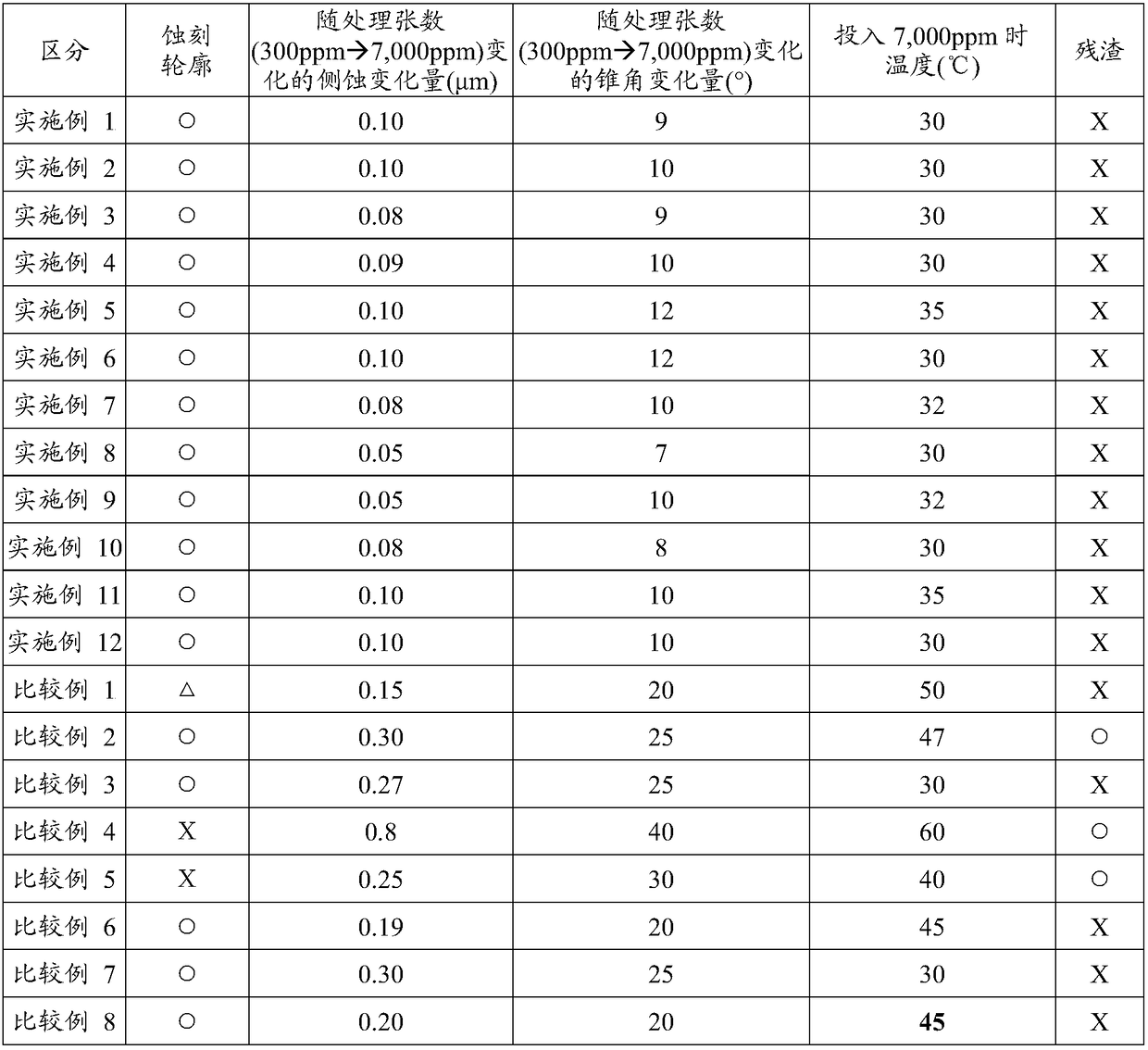
[0116] Experimental example 1. Etching profile measurement
[0117] Put the etching solution compositions of the above-mentioned Examples 1 to 12 and Comparative Examples 1 to 8 respectively in the experimental equipment (model name: ETCHER (TFT), SEMES company) of the jet etching method, and set the temperature of the etching solution composition to It is about 33°C and heated. The total etching time can be changed according to the etching temperature, and it usually takes about 50 to 80 seconds in the LCD etching process.
[0118] After placing the substrate, start spraying. When the etching time reaches 50 to 80 seconds, the substrate is taken out and cleaned with deionized water, and then dried with a hot air drying device. After cleaning and drying, the board|substrate was cut|disconnected, and the cross-section was measured using the scanning electron microscope (SEM: Hitachi company product, model name S-4700). The results are described in Table 2 below.
[0119] ...
experiment example 2
[0124] Experimental example 2. Measurement of side etch and taper angle with changes in the number of substrates processed
[0125] Put the etching solution compositions of the above-mentioned Examples 1 to 12 and Comparative Examples 1 to 8 respectively in the experimental equipment (model name: ETCHER (TFT), SEMES company) of the jet etching method, and set the temperature of the etching solution composition to It is about 33°C and heated. The total etching time can be changed according to the etching temperature, and it usually takes about 50 to 80 seconds in the LCD etching process.
[0126] Regarding the measurement of the change in side erosion and the measurement of the taper angle according to the number of substrates processed, the Mo-Ti contained in the film quality is injected in such a way that the etching solution composition changes with the metal concentration (ppm) in the substrate etching composition. and Cu powder. In the case of 300ppm, 30ppm of Mo-Ti po...
experiment example 3
[0131] Experimental example 3. Measurement of the exothermic temperature of the etchant composition varying with the number of sheets processed
[0132] Put the etching solution compositions of the above-mentioned Examples 1 to 12 and Comparative Examples 1 to 8 respectively in the experimental equipment (model name: ETCHER (TFT), SEMES company) of the jet etching method, and set the temperature of the etching solution composition to It is about 33°C and heated. The total etching time can be changed according to the etching temperature, and it usually takes about 50 to 80 seconds in the LCD etching process.
[0133] Spraying was started after placing the substrate, and the temperature of the composition at which the concentration of copper ions in the etching solution composition was 7,000 ppm was measured and described in 2 below.
PUM
| Property | Measurement | Unit |
|---|---|---|
| electrical resistivity | aaaaa | aaaaa |
Abstract
Description
Claims
Application Information