Structure and manufacturing method of third-order distributed feedback terahertz quantum cascade laser
A quantum cascade, terahertz technology, applied in lasers, phonon exciters, laser components, etc., can solve the problems of large far-field divergence angle, phase mismatch, far-field spot difference, etc., to overcome the far-field divergence The effect of large angle and large coupling power
- Summary
- Abstract
- Description
- Claims
- Application Information
AI Technical Summary
Problems solved by technology
Method used
Image
Examples
Embodiment 1
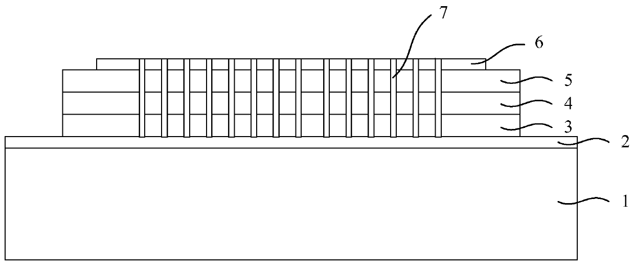
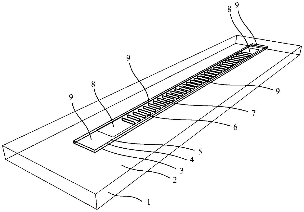
[0051] In order to solve the phase mismatch problem of the third-order distributed feedback terahertz quantum cascade laser, the present invention proposes a manufacturing scheme of a terahertz quantum cascade laser with high output power and small far-field divergence angle by changing the structure of the waveguide. see Figure 1a and Figure 1b , which are respectively shown as a cross-sectional schematic diagram and a three-dimensional schematic diagram of the third-order distributed feedback terahertz quantum cascade laser structure of the present invention, including a substrate 1, a ridge waveguide region formed on the substrate 1, and a ridge waveguide region formed on the ridge waveguide region The third-order grating structure in 7; where:
[0052] The ridge waveguide region sequentially includes a lower electrode 2, an interlayer region and an upper electrode 6 from bottom to top;
[0053] The interlayer region sequentially includes a lower contact layer 3, an acti...
Embodiment 2
[0070] The present invention also provides a method for manufacturing a third-order distributed feedback terahertz quantum cascade laser structure, including the following steps:
[0071] Step S1 is first performed: a substrate is provided, and an etch barrier layer, an upper contact layer, an active region, a lower contact layer, and a first bonding metal layer are sequentially formed on the substrate from bottom to top.
[0072] As an example, the step S1 includes:
[0073] S1-1: Using a semi-insulating GaAs wafer as a substrate, grow about 400 nm thick Al on the substrate by molecular beam epitaxy (MBE) 0.5 Ga 0.5 As etch stop layer;
[0074] S1-2: MBE grows a heavily doped n-type GaAs upper contact layer with a thickness of about 400 nanometers on the etching barrier layer, and its function is to make the metal and GaAs form a non-alloy ohmic contact;
[0075] S1-3: MBE growing an AlGaAs / GaAs alternating multilayer periodic structure active region on the contact layer, ...
PUM
 Abstract
Description
Claims
Application Information


