Resistive thin-film memory and preparation method thereof

A technology of resistive switching film and memory, which is applied in the direction of electrical components, etc., can solve the problems of the performance consistency of the resistive switching unit, the inability to pre-control the area, and the randomness of the conductive channel, so as to achieve improved performance and superior performance. Good control and consistency

Inactive Publication Date: 2017-06-30
UNIV OF ELECTRONICS SCI & TECH OF CHINA
View PDF6 Cites 6 Cited by
  • Summary
  • Abstract
  • Description
  • Claims
  • Application Information

AI Technical Summary

Problems solved by technology

However, none of the above methods can well control the distribution area of ​​defects (mainly oxygen vacancies), which will make the formation of conductive channels have great randomness, so that the resistance switching characteristics of the resistance switching unit have a certain degree of randomness. , which will have a great impact on the consistency of the performance of different resistive variable units
In addition to the oxygen vacancies mentioned above, other active metal ions such as silver ions will also form conductive filaments in the oxide film with good insulation under the action of an electric field, resulting in the phenomenon of resistance change. The introduction of ions mainly depends on the active metal used as the upper electrode material. Under the action of an electric field, the active metal undergoes a process of oxidation and then reduction, and accumulates to form a conductive channel. The above methods cannot pre-control the particle distribution area well, which is will make the formation of conductive channels very random

Method used


Image

  • Resistive thin-film memory and preparation method thereof
  • Resistive thin-film memory and preparation method thereof
  • Resistive thin-film memory and preparation method thereof

Examples


Embodiment 1

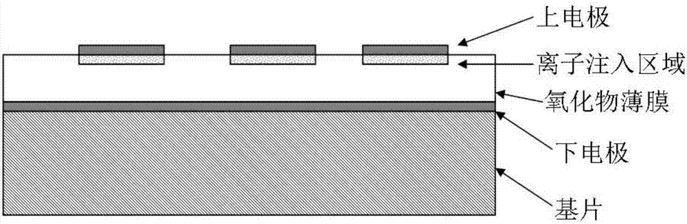
[0023] Step 1. Select a silicon substrate with a platinum electrode, and prepare a lithium niobate film with a thickness of 300 nm on one side of the platinum electrode.

[0024] Step 2, setting the locally implanted area as a photolithography mask with three circular areas with a diameter of 50 μm.

[0025] Step 3. Use the photolithography mask in step 2 to complete the photolithographic patterning process, so that the local area where the film needs to be injected (a circular area with a diameter of 50 μm) is not covered by photoresist, while the rest of the film is covered with light. Etch cover.

[0026] Step 4. Use the ions emitted by the argon ion source to perform ion implantation on the side of the silicon substrate covered with photoresist. The implantation depth is 50nm. At this time, the photoresist acts as a protective mask. Ion implantation is only possible in localized regions of the film covered with glue.

[0027] Step 5, using a sputtering method to first pr...

Embodiment 2

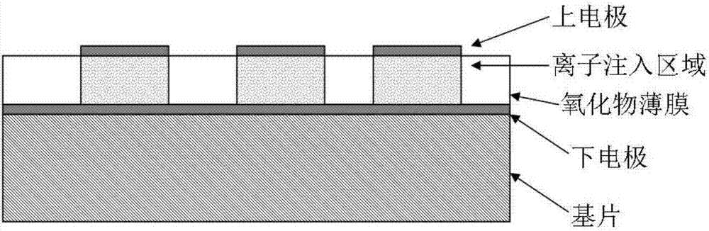
[0029] Step 1. Select a silicon substrate with a platinum electrode, and prepare a lithium niobate film with a thickness of 300 nm on one side of the platinum electrode.

[0030] Step 2, setting the locally implanted area as a photolithography mask with three circular areas with a diameter of 50 μm.

[0031] Step 3. Use the photolithography mask in step 2 to complete the photolithographic patterning process, so that the local area where the film needs to be injected (a circular area with a diameter of 50 μm) is not covered by photoresist, while the rest of the film is covered with light. Etch cover.

[0032] Step 4. Use the ions emitted by the argon ion source to perform ion implantation on the side of the silicon substrate covered with photoresist. The implantation depth is 300nm. At this time, the photoresist acts as a protective mask. Ion implantation is only possible in localized regions of the film covered with glue.

[0033] Step 5, using a sputtering method to first p...

Embodiment 3

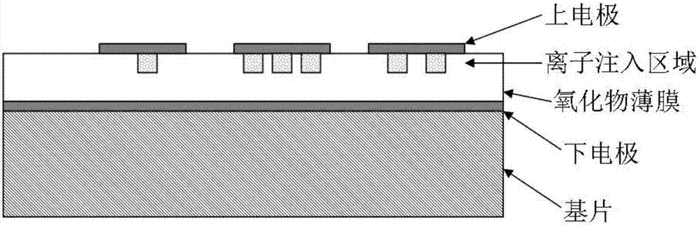
[0035] Step 1. Select a silicon substrate with a platinum electrode, and prepare a lithium niobate film with a thickness of 300 nm on one side of the platinum electrode.

[0036] Step 2, setting the locally implanted area as a photolithography mask of six circular areas with a diameter of 10 μm.

[0037] Step 3. Use the photolithography mask in step 2 to complete the photolithographic patterning process, so that the local area where the film needs to be injected (a circular area with a diameter of 10 μm) is not covered by photoresist, while the rest of the film is covered with light. Etch cover.

[0038] Step 4, using the ions emitted by the argon ion source to perform ion implantation on the side covered with photoresist, and the implantation depth is 200nm. At this time, only the film in the local area not covered by photoresist can have ion implantation.

[0039] Step 5. Set the area of ​​the upper electrode as a photolithographic mask with three square areas with a side l...


PUM

PropertyMeasurementUnit
thicknessaaaaaaaaaa

Abstract

The invention belongs to the electronic thin film and component technical field and relates to a resistive thin-film memory and a preparation method thereof. According to the resistive thin-film memory and the preparation method thereof of the invention, regions of ion implantation are controlled, so that defects can be introduced into pattern regions which are consistent with photolithographic masks; the growth of a conductive filament which plays a key role in resistive behaviors is controlled in a predetermined range, so that the controllability of the resistive performance of resistive units and the consistency of the performance of different resistive units can be greatly improved; and the shape, size, number and position of the ion implantations can be controlled, so that other functions can be realized in non implantation regions. With the resistive thin-film memory and the preparation method thereof of the invention adopted, the performance of the resistive units can be well adjusted, the resistive performance of the resistive units can be improved, at the same time, the consistency of the different resistive units on the same thin film can be improved, and a conductive filament type resistive memory which is excellent in controllability performance, simple in production process and good in consistency can be prepared.

Description

technical field [0001] The invention belongs to the technical field of electronic thin films and components, in particular to a resistive variable thin film memory and a preparation method thereof. Background technique [0002] Resistive Random Access Memory (RRAM) has become a potential non-volatile memory because of its high storage density, low power consumption, high read / write rate, simple structure and easy miniaturization. The resistive random access memory is based on the resistive characteristic of the material and uses the resistance change of the resistive unit to realize the storage of data. The resistive layer of resistive memory is generally dominated by transition metal oxide films, including titanium oxide, hafnium oxide, tantalum oxide, zirconium oxide, bismuth ferrite, lithium niobate, strontium titanate, etc., in addition to sulfide films and nitride films. [0003] Previous studies have shown that defects such as oxygen vacancies play an important role ...

Claims


Application Information

Patent Timeline
Patent Type & Authority Applications(China)
IPC IPC(8): H01L45/00
CPCH10N70/8836H10N70/043
Inventor 帅垚潘忻强吴传贵罗文博孙翔宇
Owner UNIV OF ELECTRONICS SCI & TECH OF CHINA
Why Eureka
Try Eureka