CD4069UB-based back-up power source inverter
A backup power supply and inverter technology, which is applied in the direction of electrical components, output power conversion devices, AC power input conversion to DC power output, etc., can solve the problem that square wave inverters cannot carry inductive loads, etc., and reach the scope of application wide, response speed improvement, noise reduction effect
- Summary
- Abstract
- Description
- Claims
- Application Information
AI Technical Summary
Problems solved by technology
Method used
Image
Examples
Embodiment 1
[0012] like figure 1 as shown, figure 1 It is a block diagram of the principle of the present invention. It can be seen from the figure that the inverter circuit adopts a simple one-time inverter method. The square wave generating circuit is composed of the CD4069UB peripheral circuit, and then the square wave generating circuit is composed of the CD4069UB peripheral circuit. One of them passes through an inverter and then forms a signal inversion with the other square wave signal. The two inverted square wave signals pass through two basic common-emitter amplifier circuits composed of two triodes to amplify the voltage of the square wave signal. As an inverted square wave signal, it passes through the full-bridge inverter circuit, in which the enhanced MOSFET field effect tube is the core component; at this time, in the circuit, there are two groups of P and N channel enhanced MOSFET field effect tubes respectively. A full-bridge inverter circuit composed of tubes, when...
Embodiment 2
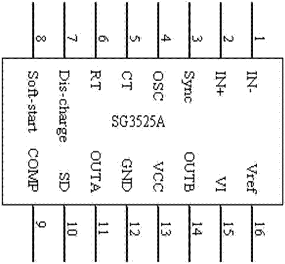
[0014] Such as figure 2 as shown, figure 2 SG3525A pin schematic diagram, is an integrated pulse width modulator produced by Silicon General (Silicon General) SG3525A is a new type of double-terminal output pulse width modulator, the operating frequency is higher than 100kHz, and the operating temperature is 0°C ~70℃, it is suitable to form a 100W~500W medium power push-pull output switching power supply. Pins 1 and 2 are the reverse input terminal and the same direction input terminal respectively. They all belong to the internal amplifier. Pin 1 is connected to the reference voltage output terminal. 16-pin connection, so that pin 1 is high level, pin 2 is grounded, and pin 3 is the synchronous terminal. There is only one chip here, so pin 3 is not used, pin 4 is the oscillator output, and pin 5 is connected to the oscillation capacitor and Pin 6 is connected to the oscillation resistor to determine the oscillation frequency of the internal sawtooth wave, and the resist...
PUM
 Abstract
Description
Claims
Application Information

