

Silicon-carbon negative electrode material and preparation method thereof
A negative electrode material, silicon carbon technology, applied in the field of materials, can solve the problems affecting the capacity of silicon-based materials, hindering the insertion of lithium ions and nano-silicon-based materials, and achieving the effect of reducing the hindrance effect
- Summary
- Abstract
- Description
- Claims
- Application Information
AI Technical Summary
Problems solved by technology
Method used
Image

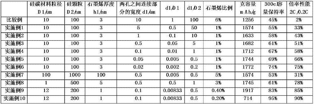
Examples
Embodiment 1
[0032] Embodiment 1 differs from Comparative Example 1 in that the present embodiment comprises the following steps:
[0033] Step 1, select the silicon particle that particle diameter is 100nm, sheet thickness is 3nm, the porous graphene sheet layer that sheet plane diameter is 50 μ m is conductive agent component (mass ratio between silicon particle and graphene is 99:1 ); the hole diameter of the porous graphene is 1 μm, and the width d1 of the continuous part between the two holes is about 5 μm;
[0034] Others are the same as those of Comparative Example 1 and will not be repeated here.
Embodiment 2
[0035] Embodiment 2 is different from Embodiment 1 in that this embodiment includes the following steps:
[0036] Step 1, select the silicon particle that particle diameter is 100nm, sheet thickness is 3nm, the porous graphene sheet layer that sheet plane diameter is 50 μ m is conductive agent component (mass ratio between silicon particle and graphene is 99:1 ); the hole diameter of the porous graphene is 1 μm, and the width d1 of the continuous part between the two holes is about 1 μm;
[0037] Others are the same as in Example 1, and will not be repeated here.
Embodiment 3
[0038] Embodiment 3 is different from Embodiment 1 in that this embodiment includes the following steps:
[0039] Step 1, select the silicon particle that particle diameter is 100nm, sheet thickness is 3nm, the porous graphene sheet layer that sheet plane diameter is 50 μ m is conductive agent component (mass ratio between silicon particle and graphene is 99:1 ); the hole diameter of the porous graphene is 1 μm, and the width d1 of the continuous part between the two holes is about 0.5 μm;
[0040] Others are the same as in Example 1, and will not be repeated here.
PUM
| Property | Measurement | Unit |
|---|---|---|
| Diameter | aaaaa | aaaaa |
| Sheet thickness | aaaaa | aaaaa |
| Layer thickness | aaaaa | aaaaa |
Abstract
Description
Claims
Application Information