A system and method for power detection and failure judgment

A power detection and judgment system technology, applied in the direction of electronic circuit testing, etc., can solve the problems of large output voltage jitter of power output devices, increased design cost and test time, and inability to quickly develop detection and failure judgment devices, etc.

Active Publication Date: 2019-08-13
CHIPSEA TECH SHENZHEN CO LTD
View PDF5 Cites 0 Cited by
  • Summary
  • Abstract
  • Description
  • Claims
  • Application Information

AI Technical Summary

Problems solved by technology

At present, the test platform cannot automatically detect the electrical properties and power range parameters of the I / O pins under different voltage conditions, which brings certain difficulties to the designers to analyze the problem and the comprehensiveness of the data; the test equipment with C51 as the control core, peripherals less, data acquisition accuracy and processing speed are low, and the high-speed and high-precision signal of the input power cannot be detected; affected by the tester's own skills and carefulness, under the condition of no insertion detection, the chip dislocation phenomenon during the test process Occurs from time to time, so that unnecessary time for positioning problems is increased, and in severe cases, it causes misjudgment of chip performance; the output voltage of traditional power output devices fluctuates greatly, and the output voltage cannot be effectively locked, resulting in large fluctuations in test data and data authenticity Large and repetitive work, etc.; online programming cannot be performed, and an external recorder needs to be purchased to remove the chip for programming each time, which is not conducive to program update, low work efficiency and heavy workload; cannot simultaneously perform multi-index item failure Detection, such as IOH / IOL, VIL / VIH, VOL / VOH, power consumption and leakage and other parameters for detection, each measurement requires a separate equipment, low efficiency and high time cost, seriously affecting the customer's production and testing progress
[0003] At present, the existing detection devices are independent and cannot perform multiple failure detections at the same time. The detection device based on the 8-bit MCU architecture has a single function, few internal peripherals, small program and data storage space, and low chip operating frequency. The coupling between them is too strong, low-density and high-coupling, resulting in simple software layered design, low program modularization and reusability design, unable to quickly develop new detection and failure judgment devices, unstable input signals lead to unreliable data, The repetitive workload is heavy, and there is no complete detection and discrimination device for the problem detection equipment due to the failure of the chip's electrical characteristics, and the power detection and failure analysis cannot be performed at the same time. The test brings great time difficulties. The whole process requires human participation. A large number of repetitive work increases the cost of manpower, material and time resources. High internal friction leads to high test costs. The lack of integration of testing results in increased hardware costs. The difficulty of maintenance is increased; relying on the skills and care of the testers themselves will have a certain impact on the function and performance of the chip test, and in severe cases, the testers will misjudge the problem, increasing the design cost and testing time; The detection equipment is inconvenient to carry, and cannot be effectively used for customers and tests, and the detection and failure judgment on the client side are limited; the traditional detection method requires a lot of human operations, and the analysis of failure items is single, which will be restricted by actual conditions. It cannot be effectively discriminated, lacks a device that integrates composite detection and failure discrimination, and can only rely on external instruments and equipment for manual analysis alone, which is inefficient

Method used


Image

  • A system and method for power detection and failure judgment
  • A system and method for power detection and failure judgment
  • A system and method for power detection and failure judgment

Examples


Embodiment Construction

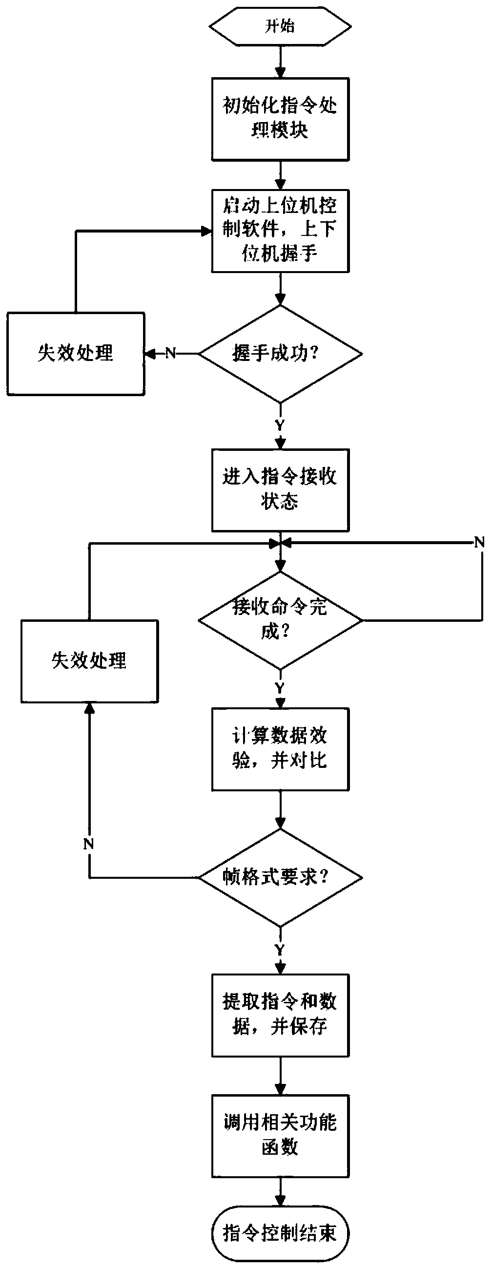
[0051] In order to make the object, technical solution and advantages of the present invention clearer, the present invention will be further described in detail below in conjunction with the accompanying drawings and embodiments. It should be understood that the specific embodiments described here are only used to explain the present invention, not to limit the present invention.

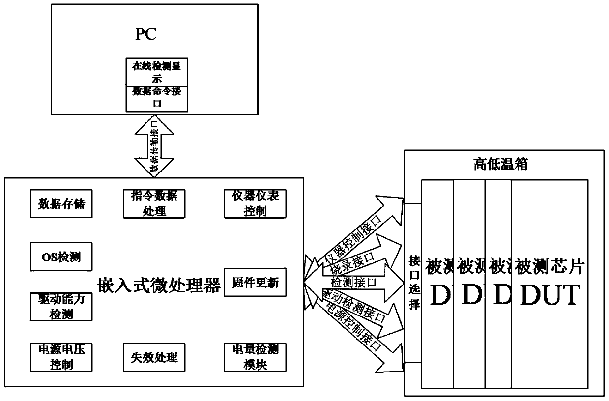
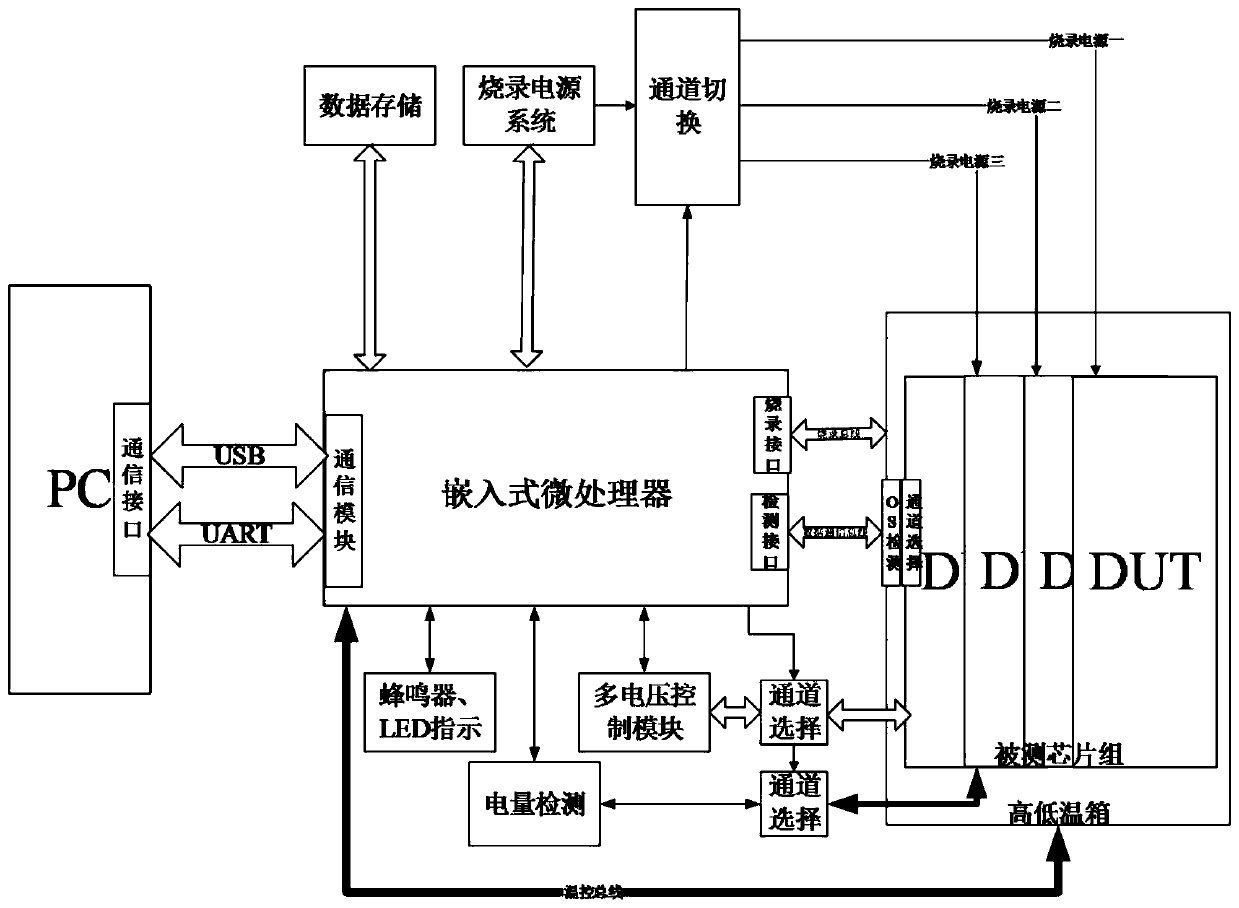
[0052] see figure 1 , 2 As shown, the present invention realizes the power detection and failure judgment system of the chip. The system integrates multiple power and electrical indicators into a system for detection and failure judgment, including the physical and electrical connection characteristics of the chip itself, which greatly improves work efficiency. And according to the relevant issues for analysis and instructions. The system consists of command processing module, data storage module, OS detection module, power control module, voltage self-calibration module, firmware update module, ...


PUM


Abstract

The invention discloses an electric quantity detection and failure determination system, and an electric quantity detection and failure determination system method. The electric quantity detection and failure determination system comprises a command processing module, a data storage module, an OS detection module, a power supply control module, a voltage self-calibration module, a firmware update module, a driving capability detection module, an electric quantity detection module and a failure detection module. The system and the method disclosed by the invention integrate multiple electric quantity and electrical indexes, including physical and electrical connection features of a chip, in a set of system for conducting detection and failure determination, significantly improve the working efficiency, and carry out analysis and instruction according to relevant problems; and the entire detection and failure determination process is carried out automatically, and the degree of automation is high.

Description

technical field [0001] The invention belongs to the technical field of chip testing, and in particular relates to a device for testing and failure judging the voltage and current characteristics of the input and output of chip IO pins, leakage and power consumption, etc. based on an embedded microprocessor. Background technique [0002] In order to meet the application needs of chip power testing and failure judgment in the R&D testing stage, and at the same time consider the integration, reliability and durability of the detection system, the application scenarios of power performance indicators of chip products have put forward very high requirements. At present, the test platform cannot automatically detect the electrical properties and power range parameters of the I / O pins under different voltage conditions, which brings certain difficulties to the designers to analyze the problem and the comprehensiveness of the data; the test equipment with C51 as the control core, per...

Claims


Application Information

Patent Timeline
Patent Type & Authority Patents(China)
IPC IPC(8): G01R31/28
CPCG01R31/28
Inventor 庞新洁
Owner CHIPSEA TECH SHENZHEN CO LTD
Why Eureka
Try Eureka