A germanium silicon channel fin field effect transistor and its preparation method

A fin field effect, germanium-silicon channel technology, applied in semiconductor/solid-state device manufacturing, semiconductor devices, electrical components, etc., can solve the problems of poor heat dissipation and high cost of devices, reduce area, improve heat dissipation problems, reduce cost effect

Active Publication Date: 2020-04-03
PEKING UNIV
View PDF3 Cites 0 Cited by
  • Summary
  • Abstract
  • Description
  • Claims
  • Application Information

AI Technical Summary

Problems solved by technology

[0003] At present, silicon germanium channel FinFETs are mainly implemented on SGOI substrates, but since the thermal conductivity of the silicon oxide buried oxide layer is about 1% of that of silicon, the device has poor heat dissipation and high cost

Method used


Image

  • A germanium silicon channel fin field effect transistor and its preparation method
  • A germanium silicon channel fin field effect transistor and its preparation method
  • A germanium silicon channel fin field effect transistor and its preparation method

Examples


Embodiment Construction

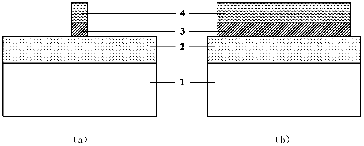
[0031] The invention forms a BOI structure through thermal oxidation, cuts off the leakage current channel between the source and the drain, can effectively suppress the leakage current of the device, and has a smaller buried oxide layer area than the SGOIFinFET, which can improve the heat dissipation effect. In addition, the use of germanium aggregation technology in the oxidation process is beneficial to increase the germanium composition in the channel, improve carrier mobility, and thus increase the on-state current. The present invention will be described in detail below in conjunction with the accompanying drawings.

[0032] A silicon germanium channel BOIFinFET can be realized according to the following steps:

[0033] Step 1. MBE grows a 50nm silicon germanium epitaxial layer 2 on a P-type (100) silicon substrate 1, deposits silicon oxide by PECVD, forms an active region by photolithography and RIE etching, and removes the glue;

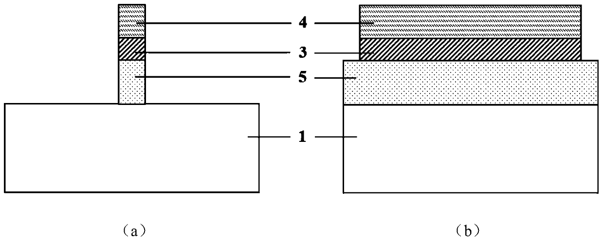
[0034] Step 2. Deposit a 30nm silicon...


PUM

PropertyMeasurementUnit
thicknessaaaaaaaaaa
thicknessaaaaaaaaaa
widthaaaaaaaaaa

Abstract

The invention discloses a germanium-silicon channel fin type field effect transistor and a preparation method thereof. According to the germanium-silicon channel fin type field effect transistor, a body-on-insulator (BOI) structure is formed through thermal oxidation; a current leakage channel between a source and a drain is cut off; a leakage current of a device can be effective suppressed; the buried oxide layer area of the germanium-silicon channel fin type field effect transistor is smaller than that of an SGOI FinFET; and a heat dissipation effect can be improved. Moreover, in an oxidization process, a germanium accumulation technology is beneficial for improving a germanium component in a channel; the carrier mobility is improved; and an on state current is improved.

Description

technical field [0001] The invention relates to a germanium-silicon channel fin field effect transistor and a preparation method thereof, belonging to the technical field of ultra-large-scale integrated circuit manufacturing. Background technique [0002] With the rapid development of integrated circuits, the feature size of semiconductor devices continues to shrink. When the feature size of the device enters the nanoscale field, due to the limitations of physical mechanism and process technology, traditional silicon-based planar devices face serious problems such as short channel effect and mobility degradation. In order to solve these problems, device structures such as double-gate and multi-gate have been proposed, and high-mobility channel materials have been introduced to improve device performance. Fin field effect transistor (FinFET) can effectively suppress the short channel effect, and has the advantages of good gate control ability, large on-state current, and com...

Claims


Application Information

Patent Timeline
Patent Type & Authority Patents(China)
IPC IPC(8): H01L29/78H01L21/336
CPCH01L29/66795H01L29/785
Inventor 安霞张冰馨胡向阳黎明黄如张兴
Owner PEKING UNIV
Why Eureka
Try Eureka