Epitaxial structure of ultraviolet light emitting diode and preparation method thereof

A technology of light-emitting diodes and epitaxial structures, applied in semiconductor devices, electrical components, circuits, etc., can solve the problems of difficult material preparation, increased mobility, and low yield of ultraviolet LEDs, and achieves improved light output power and luminous efficiency. The effect of reducing dislocation density and improving crystal quality

Inactive Publication Date: 2017-07-14
WUHAN UNIV
View PDF1 Cites 5 Cited by
  • Summary
  • Abstract
  • Description
  • Claims
  • Application Information

AI Technical Summary

Problems solved by technology

[0004] At present, the epitaxial growth technology of ultraviolet LED is not mature enough, and it is difficult to prepare materials for growing high-performance ultraviolet LED
AlN is the most suitable substrate for epitaxial high Al composition AlGaN and the preparation of ultraviolet LEDs due to its high thermal conductivity and high UV transparency, and the small lattice mismatch with high Al composition AlGaN materials. However, AlN bulk materials exist great difficulty
In addition, the hole concentration of the p-type AlGaN material with high Al composition is extremely low, and the increase of the compensation center and the scattering center causes its mobility to decrease, which makes the conductivity of the P-type AlGaN material extremely low, and cannot be combined with metal The electrodes form a good ohmic contact, necessitating the use of P-type GaN as the topmost electrode contact layer
However, since GaN strongly absorbs ultraviolet rays, the efficiency of emitting light from the front is very low.
Moreover, the current UV LED growth technology is not mature enough, and the dislocation density in the epitaxial structure greatly limits the luminous efficiency of UV LEDs. These reasons lead to the low luminous efficiency of UV LED chips, high cost and difficulty in preparation low yield

Method used


Image

  • Epitaxial structure of ultraviolet light emitting diode and preparation method thereof
  • Epitaxial structure of ultraviolet light emitting diode and preparation method thereof
  • Epitaxial structure of ultraviolet light emitting diode and preparation method thereof

Examples


Embodiment 1

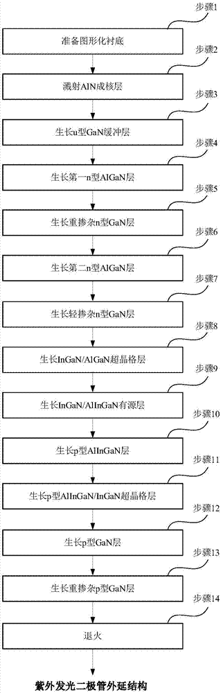
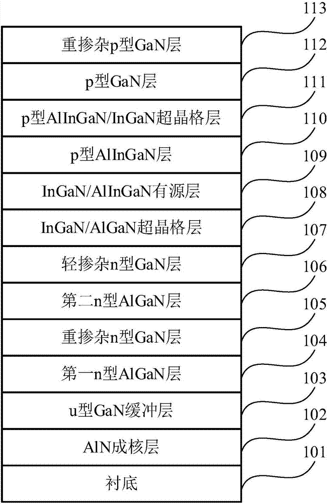
[0026] Such as figure 1 As shown, the method for preparing the epitaxial structure of the ultraviolet light emitting diode provided in the first embodiment includes the following steps:

[0027] Step 1. Prepare the patterned substrate:

[0028] Using photoresist reflow and inductively coupled plasma technology (ICP) to make a patterned substrate, specifically: first heat the photoresist mask to form a trapezoidal structure, and then use inductively coupled plasma The etching method etches a cone shape;

[0029] Step 2. Sputtering AlN nucleation layer:

[0030] Place the cleaned patterned substrate on a rotatable substrate, then place an aluminum target with a purity of 99.99% on the copper back plate of the reactive magnetron sputtering equipment, and draw the coating chamber into 2.5×10 -3 In the Pa vacuum chamber, pass high-purity inert gas Ar (99.999%), and start sputtering Al target at the same time, select RF power 13.65MHZ, control the sputtering rate of Al target to 5nm / min, at...

Embodiment 2

[0058] Such as figure 1 As shown, the method for preparing the epitaxial structure of the ultraviolet light emitting diode provided in the second embodiment includes the following steps:

[0059] Step 1. Prepare the patterned substrate:

[0060] The patterned substrate is made by photoresist reflow and inductively coupled plasma technology, specifically: the photoresist mask is first subjected to a thermal reflow process so that the photoresist forms a trapezoidal structure, and then the inductively coupled plasma is used for etching Method to etch a cone shape;

[0061] Step 2. Sputtering AlN nucleation layer:

[0062] Place the cleaned patterned substrate on a rotatable substrate, then place an aluminum target with a purity of 99.99% on the copper back plate of the reactive magnetron sputtering equipment, and draw the coating chamber into 2.5×10 -3 In the Pa vacuum chamber, pass high-purity inert gas Ar (99.999%), and start sputtering Al target at the same time, select RF power 13.6...

Embodiment 3

[0089] The method for preparing the epitaxial structure of the ultraviolet light emitting diode provided in the third embodiment includes the following steps:

[0090] Step 1. Prepare the patterned substrate:

[0091] The patterned substrate is made by photoresist reflow and inductively coupled plasma technology, specifically: the photoresist mask is first subjected to a thermal reflow process so that the photoresist forms a trapezoidal structure, and then the inductively coupled plasma is used for etching Method to etch a cone shape;

[0092] Step 2. Sputtering AlN nucleation layer:

[0093] Place the cleaned patterned substrate on a rotatable substrate, then place an aluminum target with a purity of 99.99% on the copper back plate of the reactive magnetron sputtering equipment, and draw the coating chamber into 2.5×10 -3 In the Pa vacuum chamber, pass high-purity inert gas Ar (99.999%), and start sputtering Al target at the same time, select RF power 13.65MHZ, control the sputtering...


PUM


Abstract

The invention provides an epitaxial structure of an ultraviolet light emitting diode capable of effectively improving the light output power and luminous efficiency and a preparation method thereof. The epitaxial structure of the ultraviolet light emitting diode is characterized by orderly comprising the following substances from bottom to up: a substrate, an AlN nucleating layer, a u-type GaN buffer layer, a first n-type AlGaN layer, a heavily-doped n-type GaN layer, a second n-type AlGaN layer, a lightly-doped n-type GaN layer, an InGaN/AlGaN superlattice layer, an InGaN/AlInGaN active layer, a p-type AlInGaN layer, a p-type AlInGaN/InGaN superlattice layer, a p-type GaN layer, and a heavily-doped p-type GaN layer, wherein the thickness of the first n-type AlGaN layer is 60 to 100nm, and the thickness of the second n-type AlGaN layer is 20 to 50nm.

Description

Technical field [0001] The invention belongs to the field of semiconductor optoelectronics, and specifically relates to an ultraviolet light emitting diode epitaxial structure and a preparation method thereof. [0002] technical background [0003] With the in-depth research on LED technology, people gradually shift their focus to ultraviolet LEDs with high Al component group III nitrides as structural materials. Compared with traditional ultraviolet light sources (such as mercury lamp and xenon lamp), ultraviolet LED has the advantages of environmental protection, non-toxic, low power consumption, controllable wavelength, integration, small size and long life, which is in line with environmental protection, zero pollution, and energy saving in the new era. And so on. And UV LED has great application value in medical treatment, sterilization, printing, lighting and data storage. In addition, the use of solar-blind ultraviolet light (wavelength less than 280nm) for communication c...

Claims


Application Information

Patent Timeline
Patent Type & Authority Applications(China)
IPC IPC(8): H01L33/04H01L33/06H01L33/00
CPCH01L33/04H01L33/0075H01L33/06
Inventor 周圣军高艺霖胡红坡刘星童刘梦玲
Owner WUHAN UNIV
Why Eureka
Try Eureka