LED epitaxial structure with high light extraction efficiency and growing method thereof

A technology of light extraction efficiency and epitaxial structure, applied in the field of electronics, can solve the problems of weak antistatic ability of LED devices, large dislocation density of GaN materials, weakened antistatic ability, etc., to improve antistatic ability, improve light efficiency, improve The effect of compound chance

Inactive Publication Date: 2017-08-18
XIANGNENG HUALEI OPTOELECTRONICS
View PDF5 Cites 10 Cited by
  • Summary
  • Abstract
  • Description
  • Claims
  • Application Information

AI Technical Summary

Problems solved by technology

This method can improve the light extraction efficiency to a certain extent, but it has the following defects: (1) because InN / Si y Ga (1-y) There is a large lattice mismatch between N material and GaN material, and the impact is that the dislocation density of GaN material is as high as 80 pieces / cm 2 ; (2) Because the dislocation density of GaN material is large and the crystal quality is poor, which provides a leakage channel, the antistatic ability of LED devices is relatively weak, especially under high voltage, the antistatic ability is sharply weakened

Method used


Image

  • LED epitaxial structure with high light extraction efficiency and growing method thereof
  • LED epitaxial structure with high light extraction efficiency and growing method thereof
  • LED epitaxial structure with high light extraction efficiency and growing method thereof

Examples


Embodiment 1

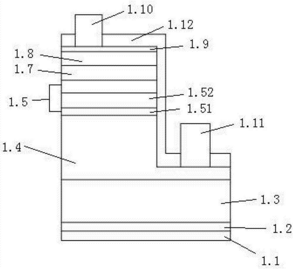
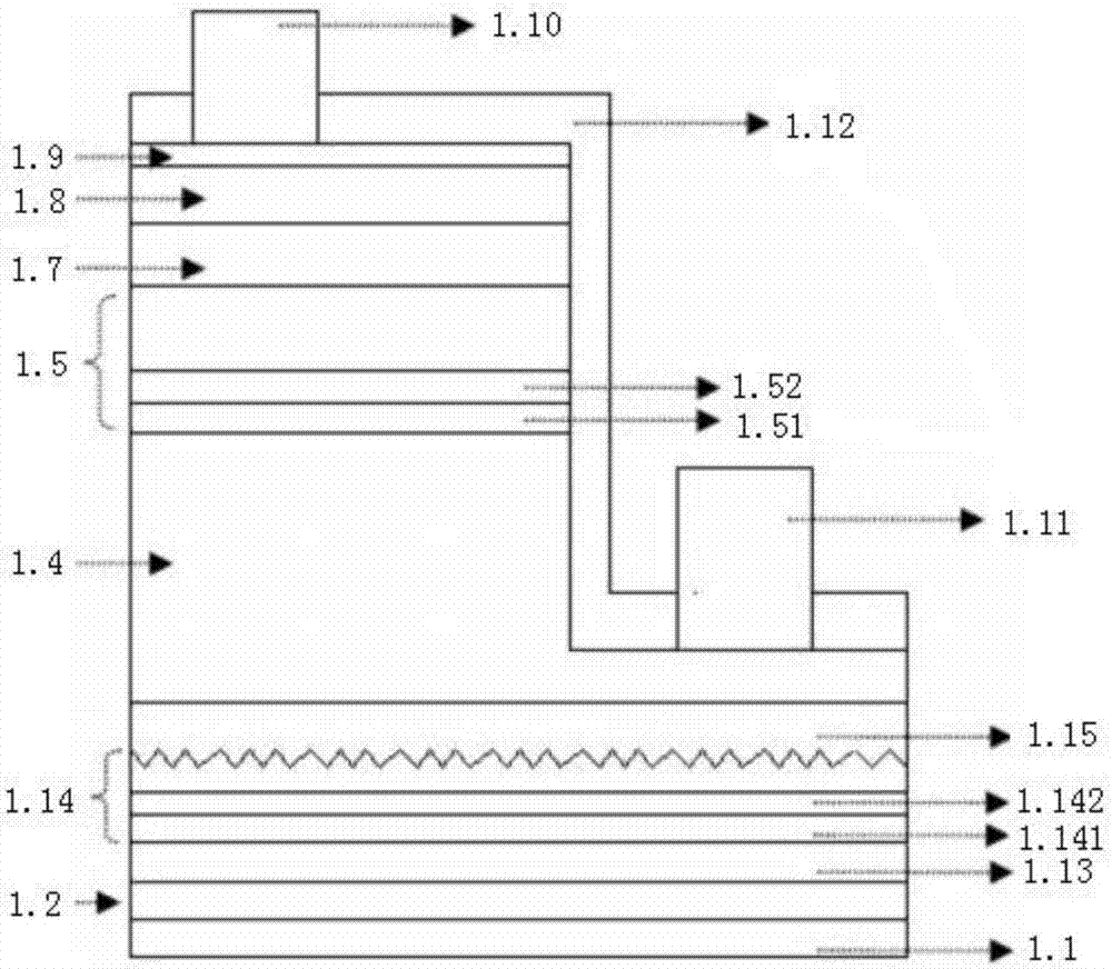
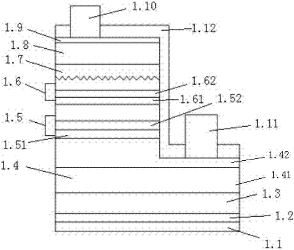
[0045] see image 3 , an LED epitaxial structure with high light extraction efficiency, sequentially stacked sapphire substrate 1.1, low-temperature buffer layer 1.2, undoped GaN layer 1.3, Si-doped n-type GaN layer 1.4, In x Ga (1-x) N / GaN light emitting layer 1.5, InN / Mg 3 N 2 A roughened layer 1.6 in the superlattice, a p-type AlGaN layer 1.7 and a magnesium-doped p-type GaN layer 1.8.

[0046] The material of the substrate 1.1 is sapphire.

[0047] The low-temperature buffer layer 1.2 is a structure corroded into irregular small islands, and its thickness is 20-40 nm.

[0048] The thickness of the undoped GaN layer 1.3 is 2-4 μm.

[0049] The Si-doped n-type GaN layer 1.4 includes a first n-type GaN layer 1.41 and a second n-type GaN layer 1.42 stacked in sequence, the thickness of the first n-type GaN layer 1.41 is 3-4 μm, Si-doped Concentration 5E18-1E19atoms / cm 3 ; The thickness of the second n-type GaN layer 1.42 is 200-400nm, and the Si doping concentration is ...

Embodiment 2- Embodiment 3

[0069] Embodiment 2-3 differs from Embodiment 1 in that: InN / Mg described in Embodiment 2 3 N 2 The roughened layer 1.6 in the superlattice includes 10 monomers stacked, the InN layer 1.61 and the Mg 3 N 2 The thickness of layer 1.62 is 2nm, InN / Mg described in embodiment 3 3 N 2 The roughened layer 1.6 in the superlattice includes 10 monomers stacked, the InN layer 1.61 and the Mg 3 N 2 Layers 1.62 are each 2.5 nm thick.

[0070] Other parameters and processing steps are all with embodiment 1.

[0071] The performance parameters of the packaged LED epitaxial structure products (labeled S2 and S3 ) obtained in Example 2-3 are shown in Table 1 for details.


PUM


Abstract

The invention provides an LED epitaxial structure which comprises a substrate, a low-temperature buffer layer, a non-doped GaN layer, an Si-doped n-type GaN layer, an InxGa(1-x)N / GaN light emitting layer, an InX / Mg3N2 super-lattice inner roughed layer, a p-type AlGaN layer and a magnesium-doped p-type GaN layer, wherein the substrate, the low-temperature buffer layer, the non-doped GaN layer, the Si-doped n-type GaN layer, the InxGa(1-x)N / GaN light emitting layer, the InX / Mg3N2 super-lattice inner roughed layer, the p-type AlGaN layer and the magnesium-doped p-type GaN layer are successively laminated. The InX / Mg3N2 super-lattice inner roughed layer comprises 8-10 monomers which are arranged in an overlapped manner. Each monomer comprises an InN layer and a Mg3N2 layer. The LED epitaxial structure provided by the invention is advantageous in that the InX / Mg3N2 super-lattice inner roughed layer covers the light emitting layer; the InX / Mg3N2 material has an advantage of low mismatch with the GaN crystal lattice; high quality of the epitaxial layer crystal is realized; not only is light efficiency improved, but also antistatic capability can be improved; and LED product quality is improved. As an integral technical solution, the InX / Mg3N2 super-lattice inner roughed layer has advantages of increasing number of photons extracted from the LED in light unit time, reducing number of attenuation times of the photons in the LED, and correspondingly improving light extraction strength. The invention further discloses a growing method of the LED epitaxial structure. The growing method of the LED epitaxial structure has advantages of concise steps, easy process parameter control and convenient industrial production.

Description

technical field [0001] The invention relates to the field of electronic technology, in particular to an LED epitaxial structure with high light extraction efficiency and a growth method thereof. Background technique [0002] At present, LED is a kind of solid-state lighting, which is recognized by consumers because of its advantages such as small size, low power consumption, long service life, high brightness, environmental protection, and durability. The driving voltage and light efficiency requirements of high-power devices are the focus of current market demand. [0003] In the prior art, the extraction of LED light generally means that photons propagate from the light-emitting layer to the surroundings of the LED at any angle, part of which is extracted from the upper and side parts of the LED, and part of which is reflected by the sapphire substrate and propagates to the surroundings again. The extraction process from the light-emitting layer to the outside; GaN on the...

Claims


Application Information

Patent Timeline
Patent Type & Authority Applications(China)
IPC IPC(8): H01L33/04H01L33/22H01L33/00
CPCH01L33/04H01L33/005H01L33/22
Inventor 徐平
Owner XIANGNENG HUALEI OPTOELECTRONICS
Why Eureka
Try Eureka