High-speed VCSEL laser epitaxial structure and preparation method therefor

An epitaxial structure and laser technology, applied in lasers, laser parts, semiconductor lasers, etc., can solve the problems of affecting device reliability, increased photon scattering loss, fast oxidation rate, etc., to reduce intrinsic parasitic capacitance, reduce The effect of scattering loss and improving product yield

Pending Publication Date: 2017-09-15
全磊光电股份有限公司
View PDF5 Cites 12 Cited by
  • Summary
  • Abstract
  • Description
  • Claims
  • Application Information

AI Technical Summary

Problems solved by technology

[0005] 1) The oxidation rate is fast, and the light exit aperture of VCSEL is difficult to control, resulting in low yield of VCSEL;
[0006] Cause: The oxidation limiting layer of traditional technology generally uses AlAs as the oxidation limiting layer. The thinner the AlAs layer is, the faster the oxidation rate is, while the oxidation pore size of VCSEL is generally 6-8um, and it is extremely difficult to stably and repeatedly control the oxidation pore size, resulting in VCSEL preparation low yield;
[0007] 2) Large parasitic capacitance affects the modulation rate of VCSEL;
[0009] 3) The stress of the oxide layer is large, and the epitaxial layer is easy to peel off after oxidation;
[0010] Cause: The AlAs oxidation limiting layer is used. Since the lattice constant of AlAs is smaller than the lattice constant of GaAs, AlAs will generate large tensile stress during growth, and the epitaxial layer will be easily peeled off after oxidation, which will affect the reliability of the device.
[0011] The above-mentioned traditional technology uses a thin oxidation-limited layer (less than 15nm), and a lens structure can be formed at the front of the oxide layer to reduce the scattering loss of photons, but it will cause the above-mentioned disadvantages
Once the thickness of the oxide layer is thickened, the front end of the oxide layer will be arc-shaped (such as figure 2 shown), the scattering loss of photons will increase, which will affect the modulation bandwidth of VCSEL

Method used


Image

  • High-speed VCSEL laser epitaxial structure and preparation method therefor
  • High-speed VCSEL laser epitaxial structure and preparation method therefor
  • High-speed VCSEL laser epitaxial structure and preparation method therefor

Examples


Embodiment 1

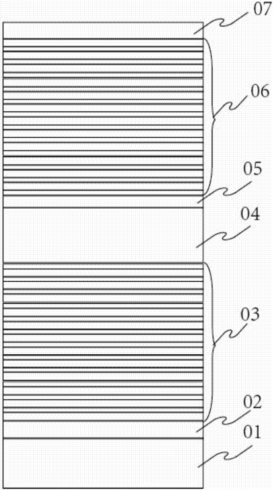
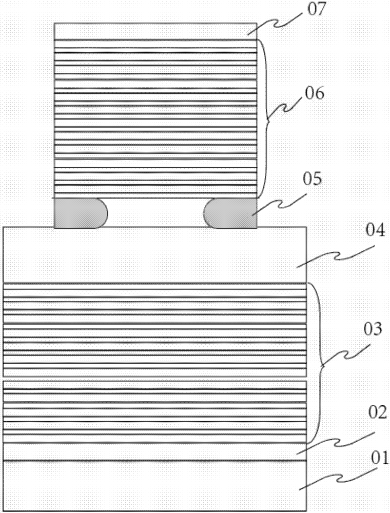
[0033] Such as figure 1 , 3 As shown, the present invention provides a high-speed VCSEL laser epitaxial structure, which includes a GaAs substrate 01, on which GaAs buffer layer 02, N-type doped DBR 03, active layer 04, oxide Confinement layer 05, P-type doped DBR06 and ohmic contact layer 07, in which the active layer 4 uses GaAs / AlGaAs MQW, and the oxidation confinement layer 05 is made of Al with multiple Ga components that can be adjusted freely 1-x Ga x As epitaxial layer composition, where X is the composition of Ga element. Multiple Al 1-x Ga x The Ga composition of the As epitaxial layer is preferably in a jump mode. The so-called jump means that the Ga composition of two adjacent epitaxial layers does not change continuously, but changes in a manner similar to a step function. As the most optimal way, multiple Al 1-x Ga x In the As epitaxial layer, the Ga component in the middle layer should be the smallest, the Ga component in the lowermost layer should be the...

Embodiment 2

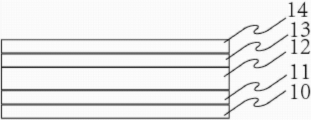
[0036] As a preferred method, the Ga composition of the middle epitaxial layer of the oxidation limiting layer is 2%, and the thickness is 10nm; the Ga composition of the lowermost and uppermost epitaxial layers is 5%, and the thickness is 5nm; The component is 2-5% and the thickness is 3-8nm. In this embodiment, the oxidation confinement layer comprises 5 nm Ga with 5% Al from bottom to top 0.95 Ga 0.05 As epitaxial layer, 3nmGa composition is 3% Al 0.97 Ga 0.03 As epitaxial layer, 10nm Ga with 2% Al 0.98 Ga 0.02 As epitaxial layer, 3nm Ga composition is 3% Al 0.97 Ga 0.03 As epitaxial layer and 5nm Ga composition with 5% Al 0.95 Ga 0.05 As epitaxial layer.

Embodiment 3

[0038] In this example, the oxidation confinement layer comprises 5nm Ga with 5% Al from bottom to top 0.95 Ga 0.05 As epitaxial layer, 8nmGa composition is 3% Al 0.97 Ga 0.03 As epitaxial layer, 10nm Ga with 2% Al 0.98 Ga 0.02 As epitaxial layer, 8nm Ga composition is 3% Al 0.97 Ga 0.03 As epitaxial layer and 5nm Ga composition with 5% Al 0.95 Ga 0.05 As epitaxial layer.

[0039] Oxidation limiting layer 05 adopts a composition hopping structure with a certain thickness. Due to the different oxidation rates of different Ga components, after it is fabricated into a VCSEL chip, its oxide layer morphology is as follows: Figure 4 shown.

[0040] In the chip process, the oxidation rate of AlGaAs increases with the decrease of the Ga composition. The oxidation limiting layer adopts AlGaAs, which has small stress and controllable oxidation rate. Therefore, compared with the traditional 30nm AlGaAs or AlAs oxidation limiting layer, the oxidation limiting layer The thicknes...


PUM


Abstract

The invention provides a high-speed VCSEL laser epitaxial structure. The laser epitaxial structure comprises a GaAs substrate; a GaAs buffer layer, an N type doped DBR, an active layer, an oxidization limiting layer, a P type doped DBR and an ohmic contact layer are deposited on the GaAs substrate by adopting MOCVD in sequence; and the oxidization limiting layer is formed by multiple Al<1-x>Ga<x>As epitaxial layers with freely adjustable Ga components, wherein X is the Ga element component. According to the laser epitaxial structure, the multiple layers of Al<1-x>Ga<x>As with certain thickness and jumping components are adopted to form the oxidization limiting layer; and the front-end shape of the oxidization limiting layer can be changed by adjusting the components in each layer of Al<1-x>Ga<x>As, so that a lens structure can be formed at the front end of the oxidization limiting layer, and photon scattering loss can be lowered, thereby improving the modulation bandwidth of the VCSEL. The laser epitaxial structure has the following advantages: 1) by adjusting the ratio of Ga in the oxidization limiting layer, the oxidization rate of the oxidization limiting layer is lowered, the oxidization can be controlled easily, and the product yield of the VCSEL chip is improved; and 2) the oxidization limiting layer is high in thickness and low in intrinsic stray capacitance.

Description

technical field [0001] The invention relates to the technical field of semiconductor optoelectronics, in particular to a high-speed VCSEL laser epitaxial structure and a preparation method thereof. Background technique [0002] Vertical cavity surface emitting laser (VCSEL) is a semiconductor laser that emits light in the direction perpendicular to the substrate on which the laser is formed. Compared with edge emitting semiconductor lasers (FP, DFB, etc.), it has small temperature drift, low threshold, and fiber coupling. High efficiency, easy integration, packaging, high speed (up and down at 100ps level) and other characteristics, it is the preferred light source in ultra-high-speed short-distance optical interconnection equipment, widely used in large-scale data centers, connections in supercomputers, and in the continuous demand for data analysis Driven by the rise, it is expected that the future output value of VCSEL will exceed one billion US dollars. Such as figure ...

Claims


Application Information

Patent Timeline
Patent Type & Authority Applications(China)
IPC IPC(8): H01S5/183
CPCH01S5/18311
Inventor 单智发
Owner 全磊光电股份有限公司
Why Eureka
Try Eureka