Light emitting diode and manufacturing method thereof

A technology for light-emitting diodes and a manufacturing method, which is applied to electrical components, circuits, semiconductor devices, etc., can solve problems such as reducing the luminous efficiency of light-emitting diode crystals, and achieve the effect of increasing the number and improving the luminous efficiency.

Active Publication Date: 2017-09-22
HC SEMITEK SUZHOU
View PDF9 Cites 11 Cited by
  • Summary
  • Abstract
  • Description
  • Claims
  • Application Information

AI Technical Summary

Problems solved by technology

[0006] In order to solve the problem in the prior art that the electron blocking layer will block a part of holes from entering the MQW layer to recombine with electrons a

Method used


Image

  • Light emitting diode and manufacturing method thereof
  • Light emitting diode and manufacturing method thereof

Examples


Embodiment 1

[0026] An embodiment of the present invention provides a light emitting diode, figure 1 It is a schematic structural diagram of a light emitting diode provided by an embodiment of the present invention, such as figure 1 As shown, the light-emitting diode includes a substrate 1, and a low-temperature buffer layer 2, a high-temperature buffer layer 3, an N-type layer 4, an active layer 5, an electron blocking layer 6, a P-type layer 7 and The activation contacts the P-type layer 8 .

[0027] Among them, the electron blocking layer 6 is composed of three sublayers, and the three sublayers include the first sublayer 61, the second sublayer 62 and the third sublayer 63 grown in sequence, and the first sublayer 61 is made of n+1 periods of AlGaN / InGaN superlattice, the second sublayer 62 is composed of n periods of AlGaN / InGaN superlattice, the third sublayer 63 is composed of n-1 periods of AlGaN / InGaN superlattice, the first sublayer 61 , the InGaN layers in the second sub-laye...

Embodiment 2

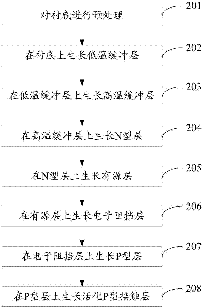
[0050] An embodiment of the present invention provides a method for manufacturing a light-emitting diode, which is suitable for the light-emitting diode provided in Embodiment 1. figure 2 It is a flowchart of a method for preparing a light-emitting diode provided by an embodiment of the present invention, such as figure 2 As shown, the manufacturing method includes:

[0051] Step 201, performing pretreatment on the substrate.

[0052] Optionally, the substrate is sapphire with a thickness of 630-650um.

[0053] In this embodiment, Veeco K465i or C4 MOCVD (Metal Organic Chemical VaporDeposition, metal organic compound chemical vapor deposition) equipment is used to realize the LED growth method. Using high-purity H 2 (hydrogen) or high-purity N 2 (nitrogen) or high purity H 2 and high purity N 2 The mixed gas as the carrier gas, high-purity NH 3 As the N source, trimethylgallium (TMGa) and triethylgallium (TEGa) are used as the gallium source, trimethylindium (TMIn) is...


PUM

PropertyMeasurementUnit
Thicknessaaaaaaaaaa
Thicknessaaaaaaaaaa
Thicknessaaaaaaaaaa

Abstract

The invention discloses a light emitting diode and a manufacturing method thereof, and belongs to the technical field of a semiconductor. An electron baffle layer of the light emitting diode comprises three sub-layers, wherein the three sub-layers comprise a first sub-layer, a second sub-layer and a third sub-layer which are sequentially grown, the first sub-layer comprises an AlGaN/InGaN superlattice layer with (n+1) periods, the second sub-layer comprises an AlGaN/InGaN superlattice layer with n periods, the third sub-layer comprises an AlGaN/InGaN superlattice layer with (n-1) periods, InGaN layers in the first sub-layer, the second sub-layer and the third sub-layer are all doped with Mg, and n is more than or equal to 3 but less than or equal to 6. The electron baffle layers are divided into three superlattice sub-layers with different doping and same structure to form three segments of baffle layers, so that non-radiative recombination due to electrons leaked to a P layer is reduced as much as possible; and moreover, the periods of the superlattices of each sub-layer in the three sub-layers are gradually reduced according to 1, the electrons can be blocked better, meanwhile, not many holes can be blocked, and the luminous efficiency of a light emitting diode crystal is further improved.

Description

technical field [0001] The invention relates to the technical field of semiconductors, in particular to a light emitting diode and a manufacturing method thereof. Background technique [0002] LED (Light Emitting Diode, Light Emitting Diode) is a semiconductor electronic component that can emit light. As an efficient, environmentally friendly and green new solid-state lighting source, it is being rapidly and widely used, such as traffic lights, car interior and exterior lights, urban landscape lighting, mobile phone backlight, etc. Improving the luminous efficiency of chips is the goal that LEDs are constantly pursuing. [0003] Existing LEDs include a substrate and an epitaxial layer stacked on the substrate. The epitaxial layer includes a low-temperature buffer layer, a high-temperature buffer layer, an N-type layer, an MQW (Multiple Quantum Well, multiple quantum well) layer, Electron blocking layer and P-type layer. Among them, the role of the electron blocking layer i...

Claims


Application Information

Patent Timeline
IPC IPC(8): H01L33/00H01L33/06H01L33/14H01L33/32
CPCH01L33/0075H01L33/06H01L33/145H01L33/325
Inventor 姚振从颖胡加辉李鹏
Owner HC SEMITEK SUZHOU
Why Eureka
Try Eureka