GaN based laser device and preparation method thereof

A technology of lasers and confinement layers, which is applied to lasers, laser components, semiconductor lasers, etc., can solve problems affecting optical power and slope efficiency, affecting optical confinement, and effective barriers of electronic blocking layers, so as to reduce optical loss and effectively Potential barrier enhancement, effect of increasing optical power and slope efficiency

Active Publication Date: 2017-09-26
INST OF SEMICONDUCTORS - CHINESE ACAD OF SCI
View PDF5 Cites 4 Cited by
  • Summary
  • Abstract
  • Description
  • Claims
  • Application Information

AI Technical Summary

Problems solved by technology

[0003] The upper waveguide layer in GaN-based violet lasers will affect the effective barrier of the opt...

Method used


Image

  • GaN based laser device and preparation method thereof
  • GaN based laser device and preparation method thereof
  • GaN based laser device and preparation method thereof

Examples


preparation example Construction

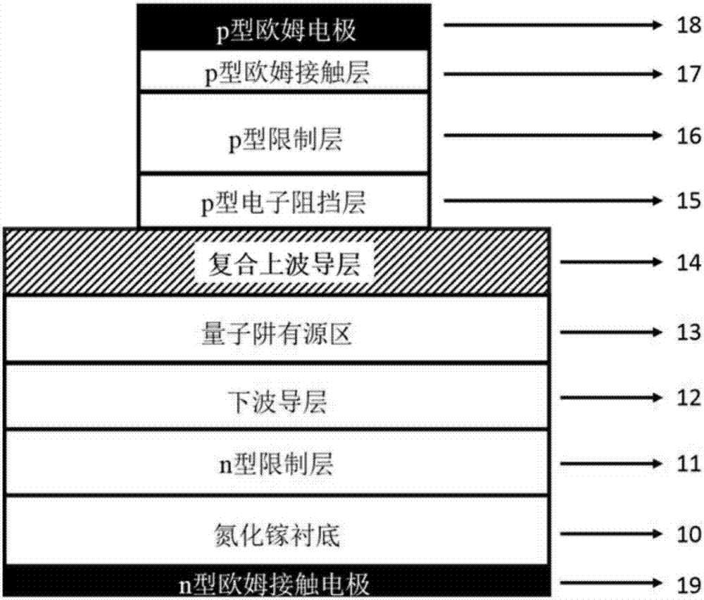
[0028] In an exemplary embodiment of the present invention, a method for manufacturing a GaN-based violet laser is provided. figure 1 It is a schematic structural diagram of a GaN-based violet laser according to an embodiment of the present invention. Such as figure 1 Shown, the preparation method of GaN-based violet laser of the present invention comprises the following steps:

[0029] S1: On the gallium nitride substrate 10, the n-type confinement layer 11, the lower waveguide layer 12, the quantum well active region 13, the composite upper waveguide layer 14, the p-type electron blocking layer 15, p-type confinement layer 16, p-type ohmic contact layer 17;

[0030] S2: Dry etching the p-type ohmic contact layer 17, the p-type confinement layer 16, the p-type electron blocking layer 15 and the composite upper waveguide layer 14 into a laser ridge shape;

[0031] S3: growing an oxide film on the formed ridge, and fabricating a p-type ohmic electrode 18 by photolithography;...


PUM

PropertyMeasurementUnit
Thicknessaaaaaaaaaa
Thicknessaaaaaaaaaa
Thicknessaaaaaaaaaa

Abstract

The invention provides a preparation method of a GaN based laser device. The preparation method comprises the following steps: S1: sequentially growing an n-type limiting layer, a lower waveguide layer, a quantum well active region, a composite upper waveguide layer, a p-type electron blocking layer, a p-type limiting layer, and a p-type ohmic contact layer on a GaN substrate; S2: etching the p-type ohmic contact layer, the p-type limiting layer, the p-type electron blocking layer and the composite upper waveguide layer to form a ridge structure of the laser device; S3: growing a layer of oxidation film on the manufactured ridge structure, and manufacturing a p-type ohmic electrode by using a photoetching method; S4: thinning and cleaning the GaN substrate, and manufacturing an n-type ohmic contact electrode on the GaN substrate; S5: splitting, coating a film, packaging on a tube shell, manufacturing the GaN based laser device with the composite upper waveguide layer, and finishing the preparation. The invention further provides the GaN based laser device. The effective potential barrier of the electron blocking layer is improved, and the laser power and the slope efficiency are improved.

Description

technical field [0001] The invention relates to the technical field of semiconductor optoelectronic devices, in particular to a GaN-based laser and a preparation method thereof. Background technique [0002] The lasing wavelength of gallium nitride-based lasers covers the entire visible light band well, and makes it have important applications in civil and military fields such as laser display, laser lighting, underwater communication, storage, etc., and has been widely studied. [0003] The upper waveguide layer in GaN-based violet lasers will affect the effective barrier of the optical confinement and electron blocking layers, which in turn will affect the optical power and slope efficiency. Contents of the invention [0004] (1) Technical problems to be solved [0005] In view of the above technical problems, the present invention provides a GaN-based laser and its preparation method, which are used to increase the effective potential barrier of the electron blocking l...

Claims


Application Information

Patent Timeline
IPC IPC(8): H01S5/343
Inventor 赵德刚梁锋
Owner INST OF SEMICONDUCTORS - CHINESE ACAD OF SCI
Why Eureka
Try Eureka