A kind of algainp semiconductor laser with superlattice confinement layer

A confinement layer and superlattice technology, which is applied in the field of AlGaInP semiconductor lasers, can solve the problems of easy diffusion and high doping of Mg atoms, etc., and achieve the effect of improving the effective barrier, reducing the probability, and preventing hot electrons from leaking into the P-type region

Active Publication Date: 2020-09-18
Shandong Huaguang Optoelectronics Co. Ltd.
View PDF7 Cites 0 Cited by
  • Summary
  • Abstract
  • Description
  • Claims
  • Application Information

AI Technical Summary

Problems solved by technology

[0006] Aiming at the problem that existing AlGaInP semiconductor lasers are not easy to be highly doped with Mg atoms and are easy to diffuse, the present invention provides an AlGaInP semiconductor laser with a superlattice confinement layer, which can obtain a steep high-concentration Mg-doped edge

Method used


Image

  • A kind of algainp semiconductor laser with superlattice confinement layer
  • A kind of algainp semiconductor laser with superlattice confinement layer

Examples


Embodiment

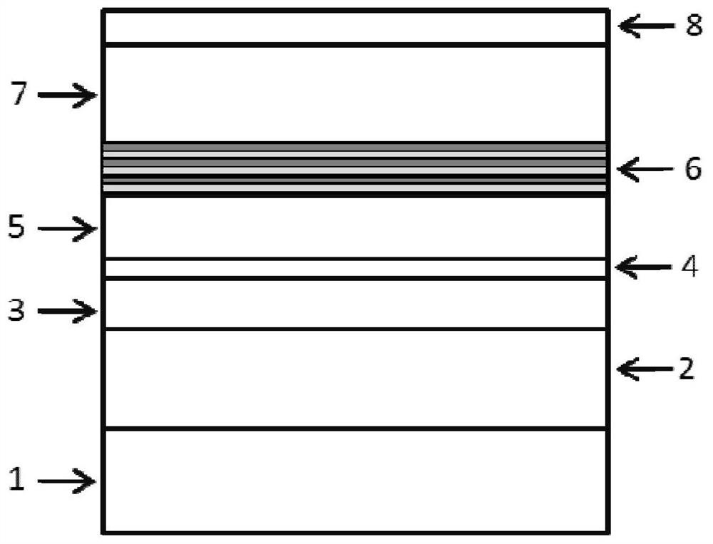
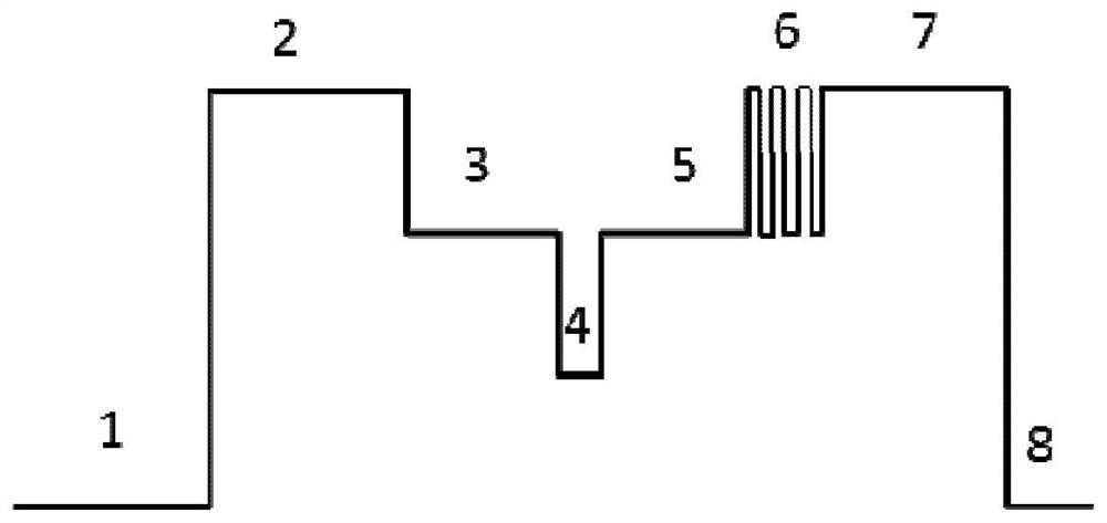
[0031] like figure 1 As shown, an AlGaInP semiconductor laser with a superlattice confinement layer comprises, from bottom to top, a substrate 1, a lower confinement layer 2, a lower waveguide layer 3, a quantum well layer 4, an upper waveguide layer 5, and a first upper confinement layer 6. The second upper confinement layer 7 and the ohmic contact layer 8 .

[0032] The substrate 1 is an N-type GaAs (100) single wafer with a biased crystal orientation, the off-angle is 10°, the N-type dopant material is Si, and the doping concentration is 3×10 18 cm -3 .

[0033] The lower confinement layer 2 is N-type (Al 0.7 Ga 0.3 ) 0.5 In 0.5 P, N type doping material is Si, doping concentration is 8×10 17 cm -3 , with a thickness of 1200nm.

[0034] The lower waveguide layer 3 is non-doped (Al 0.5 Ga 0.5 ) 0.5 In 0.5 P, with a thickness of 100 nm.

[0035] Quantum well layer 4 is Ga 0.45 In 0.55 P, the thickness is 10nm, and the lasing wavelength is 650nm.

[0036] The...


PUM

PropertyMeasurementUnit
thicknessaaaaaaaaaa
thicknessaaaaaaaaaa
thicknessaaaaaaaaaa

Abstract

The present invention relates to an AlGaInP semiconductor laser with a superlattice limiting layer. The AlGaInP semiconductor laser includes a substrate, a lower limiting layer, a lower waveguide layer, a quantum well layer, an upper waveguide layer, a first upper limiting layer, a second upper limiting layer and an ohmic contact layer from the bottom to the top. The first upper limiting layer isa superlattice structure in which an AlGaInP material of a high aluminum component and an AlGaInP material of a low aluminum component are alternately grown, in the first upper limiting layer, the doping material of the AlGaInP material of the high aluminum component is Mg, the doping material of the AlGaInP material of the low aluminum component is Mg, the second upper limiting layer is the AlGaInP material of the high aluminum component, and the doping material of the second upper limiting layer is Mg. According to the AlGaInP semiconductor laser, the highly doped first upper limiting layerand second upper limiting layer are used, the series resistance of an epitaxial layer can be reduced, the generation of Joule heat is reduced, and the photoelectric conversion efficiency is improved.

Description

technical field [0001] The invention relates to an AlGaInP semiconductor laser with a superlattice confinement layer, belonging to the technical field of semiconductor lasers. Background technique [0002] AlGaInP quaternary compound materials are widely used in high-brightness red light-emitting diodes and semiconductor lasers, and have become the mainstream materials for red light-emitting devices. However, compared with the AlGaAs material used in the early stage, the AlGaInP material system itself also has its disadvantages: the conduction band step of the AlGaInP / GaInP heterojunction is very small, with a maximum value of about 270meV, which is less than 350meV of the AlGaAs material, so the electronic barrier is relatively low , it is easy to form a leakage current, which increases the threshold current of the laser, especially in high temperature and high current work; AlGaInP material has a much higher thermal resistance than AlGaAs material due to alloy scattering, ...

Claims


Application Information

Patent Timeline
Patent Type & Authority Patents(China)
IPC IPC(8): H01S5/34H01S5/343H01S5/20
CPCH01S5/2004H01S5/34H01S5/343
Inventor 徐现刚朱振张新
Owner Shandong Huaguang Optoelectronics Co. Ltd.
Why Eureka
Try Eureka