Red light semiconductor laser with high reliability

A reliability and laser technology, applied to the structure of the active region, can solve the problems of low characteristic temperature and life, high light absorption and high junction temperature, and achieve reduced Joule heat generation, good confinement, and reduced series resistance Effect

Inactive Publication Date: 2015-01-07
Shandong Huaguang Optoelectronics Co. Ltd.
View PDF6 Cites 13 Cited by
  • Summary
  • Abstract
  • Description
  • Claims
  • Application Information

AI Technical Summary

Problems solved by technology

[0009] Aiming at the problems of existing red semiconductor lasers such as high light absorption, high junction temperature, low characteristic temperature and low lifespan, the present invention provid

Method used


Image

  • Red light semiconductor laser with high reliability
  • Red light semiconductor laser with high reliability
  • Red light semiconductor laser with high reliability

Examples


Embodiment 1

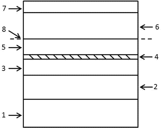
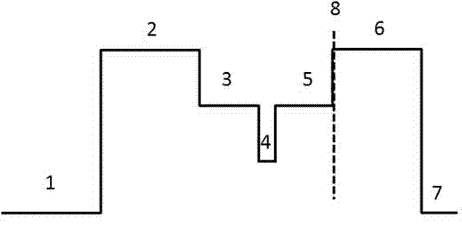
[0043] Substrate 1 is a Si-doped GaAs(100) single crystal substrate with a 15° orientation to , and the doping concentration is 3×10 18 cm -3 .

[0044] The lower confinement layer 2 is Si-doped (Al 0.7 Ga 0.3 ) 0.5 In 0.5 P, the doping concentration is 1×10 18 cm -3 .

[0045] The lower waveguide layer 3 is weakly N-type Si-doped (Al 0.5 Ga 0.5 ) 0.5 In 0.5 P, the doping concentration is 6×10 16 cm -3 .

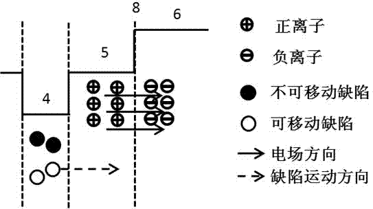
[0046] Quantum well active region 4 is Ga with a thickness of 15nm 0.5 In 0.5 p.

[0047] The upper waveguide layer 5 is weakly N-type Si-doped (Al 0.5 Ga 0.5 ) 0.5 In 0.5 P, the doping concentration is 6×10 16 cm -3 .

[0048] The upper confinement layer 6 is Mg-doped (Al 0.7 Ga 0.3 ) 0.5 In 0.5 P, the doping concentration is 2×10 18 cm -3 .

[0049] The ohmic contact layer 7 is GaAs with a thickness of 200nm, and the doping concentration of Zn is 3×10 19 cm -3 .

[0050] In this embodiment the confinement layer is (Al 0.7 Ga 0.3 ) 0.5 In...

Embodiment 2

[0052] The difference between this embodiment and the highly reliable red semiconductor laser described in Embodiment 1 is:

[0053] The lower confinement layer 2 is Se-doped Al with a thickness of 1.0 μm 0.5 In 0.5 P, the doping concentration is 1×10 18 cm -3 .

[0054] The lower waveguide layer 3 is weakly N-type Se-doped (Al 0.5 Ga 0.5 ) 0.5 In 0.5 P, the doping concentration is 8×10 16 cm -3 .

[0055] The quantum well 4 is Ga with a thickness of 10nm 0.6 In 0.4 p.

[0056] The upper waveguide layer 5 is weakly N-type Se-doped (Al 0.5 Ga 0.5 ) 0.5 In 0.5 P, the doping concentration is 8×10 16 cm -3 .

[0057] The upper confinement layer 6 is Mg-doped Al with a thickness of 1.0 μm 0.5 In 0.5 P, the doping concentration is 2×10 18 cm -3 .

[0058] The ohmic contact layer 7 is GaAs with a thickness of 200nm, and the doping concentration of C is 5×10 19 cm -3 .

[0059] In this embodiment, the confinement layer uses Al with a smaller refractive index...


PUM

PropertyMeasurementUnit
Doping concentrationaaaaaaaaaa
Widthaaaaaaaaaa

Abstract

Provided is a red light semiconductor laser with high reliability. The emission wavelength of the red light semiconductor laser with high reliability ranges from 630 nm to 690 nm. The red light semiconductor laser with high reliability structurally comprises a substrate, a lower limiting layer, a lower waveguide layer, a quantum well active area, an upper waveguide layer, an upper limiting layer and an ohmic contact layer from bottom to top in sequence. Doping is carried out on the waveguide layer on the basis of the structure of a traditional semiconductor laser, the active area is separated from a PN junction, the highfield of the PN junction will attract the movable defects of the active area, and therefore the reliability of the laser is improved. Meanwhile, the doping atoms of the upper waveguide layer can prevent the high-doping-density atoms of the upper limiting layer from being diffused to the active area, and the power attenuation of the laser during continuous working is reduced. Due to the fact that doping is carried out on the waveguide layer, the series resistance of the laser is reduced, conversion efficiency is improved, the amount of generated joule heat is reduced, and the reliability of the red light laser during long-term working is further improved.

Description

technical field [0001] The invention relates to a highly reliable red light semiconductor laser, which belongs to the technical field of semiconductor lasers. Background technique [0002] Red semiconductor lasers have the advantages of small size, long life, and high photoelectric conversion efficiency. They are gradually replacing traditional He-Ne gas lasers and ruby ​​solid-state lasers, and are widely used in optical disk reading and writing systems, barcode readers, and alignment markers. , medical care equipment and other fields. In addition, it is also a red light source for laser display devices such as laser TVs and portable projectors. These applications require the laser to maintain a stable optical mode and laser power output, and have high requirements on the life and reliability of the laser. [0003] The earliest red semiconductor lasers used AlGaAs material systems, such as 780nm AlGaAs semiconductor lasers for CD players. Since the storage density of an ...

Claims


Application Information

Patent Timeline
IPC IPC(8): H01S5/32H01S5/30
Inventor 朱振李沛旭张新蒋锴徐现刚
Owner Shandong Huaguang Optoelectronics Co. Ltd.
Why Eureka
Try Eureka