
Dicing chip Bonding Film And Method For Manufacturing Semiconductor Device

A technology for die-bonding films and dicing chips, which is used in semiconductor/solid-state device manufacturing, semiconductor devices, and thin-film/sheet-like adhesives, etc., and can solve problems such as inability to pick up properly and chips that cannot be peeled off from dicing sheets.

Inactive Publication Date: 2017-10-03
NITTO DENKO CORP
View PDF8 Cites 1 Cited by
  • Summary
  • Abstract
  • Description
  • Claims
  • Application Information

AI Technical Summary

Problems solved by technology

On the other hand, there is a problem that the chip cannot be peeled off from the dicing sheet at the time of picking up, and it may not be picked up properly.

Method used


Image

  • Dicing chip Bonding Film And Method For Manufacturing Semiconductor Device
  • Dicing chip Bonding Film And Method For Manufacturing Semiconductor Device
  • Dicing chip Bonding Film And Method For Manufacturing Semiconductor Device

Examples


Embodiment 1

[0185]

[0186] 100 parts of 2-ethylhexyl acrylate (hereinafter also referred to as "2EHA"), 2-hydroxyethyl acrylate (hereinafter also referred to as 19 parts called "HEA"), 0.4 parts of benzoyl peroxide, and 80 parts of toluene were subjected to polymerization treatment at 60° C. for 10 hours in a nitrogen stream to obtain an acrylic polymer A.

[0187] Add 1.2 parts of 2-methacryloyloxyethyl isocyanate (hereinafter also referred to as "MOI") to this acrylic polymer A, and perform addition reaction treatment at 50°C for 60 hours in an air stream to obtain acrylic polymer A. Polymer A'.

[0188] Next, 1.3 parts of a polyisocyanate compound (trade name "CORONATEL", manufactured by Nippon Polyurethane Co., Ltd.) and a photopolymerization initiator (trade name "IRGACURE 184", manufactured by Ciba Specialty Chemicals Inc.) were added to 100 parts of the acrylic polymer A'. 3 parts) to prepare a binder solution (also referred to as "binder solution A").

[0189] The adhesive so...

Embodiment 2

[0200]

[0201] The following (a) to (e) were dissolved in methyl ethyl ketone to obtain an adhesive composition solution B having a solid content concentration of 20% by weight.

[0202] (a) Acrylic resin (trade name "SG-708-6" manufactured by Nagase ChemteX Corporation, glass transition temperature (Tg): 4°C): 100 parts

[0203] (b) Epoxy resin (trade name "JER1010", manufactured by Mitsubishi Chemical Corporation, solid at 23° C.): 140 parts

[0204] (c) Epoxy resin (trade name "JER828" manufactured by Mitsubishi Chemical Corporation, liquid at 23°C): 60 parts

[0205] (d) Phenolic resin (trade name "MEH-7851ss" manufactured by Meiwa Kasei Co., Ltd., solid at 23°C): 100 parts

[0206] (e) Spherical silica (trade name "SO-25R" manufactured by Admatechs Co., Ltd.): 40 parts

[0207] The adhesive composition solution B is coated on a release-treated film (release liner) formed of a polyethylene terephthalate film with a thickness of 50 μm that has been subjected to a silic...

Embodiment 3

[0211]

[0212] The following (a) to (e) were dissolved in methyl ethyl ketone to obtain an adhesive composition solution C having a solid content concentration of 20% by weight.

[0213] (a) Acrylic resin (trade name "SG-70L" manufactured by Nagase ChemteX Corporation, glass transition temperature (Tg): -13°C): 100 parts

[0214] (b) Epoxy resin (trade name "JER1010", manufactured by Mitsubishi Chemical Corporation, solid at 23° C.): 140 parts

[0215] (c) Epoxy resin (trade name "JER828" manufactured by Mitsubishi Chemical Corporation, liquid at 23°C): 60 parts

[0216] (d) 100 parts of phenolic resin (trade name "MEH-7851ss" manufactured by Meiwa Chemical Industry Co., Ltd., solid at 23° C.)

[0217] (e) Spherical silica (trade name "SO-25R" manufactured by Admatechs Co., Ltd.): 100 parts

[0218] The adhesive composition solution C is coated on a release-treated film (release liner) formed of a polyethylene terephthalate film with a thickness of 50 μm that has been sub...


PUM

PropertyMeasurementUnit
peel strengthaaaaaaaaaa
glass transition temperatureaaaaaaaaaa
storage modulusaaaaaaaaaa

Abstract

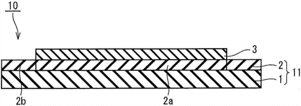
The invention discloses a dicing chip bonding film and a method for manufacturing a semiconductor device, wherein, the dicing chip bonding film can prevent a chip bonding film from floating from a dicing sheet in a cooling and expansion procedure, and can peel a semiconductor chip with the chip bonding film from the dicing sheet suitably in a picking procedure. The dicing chip bonding film comprises a dicing sheet; and a chip bonding film that is overlapped on the dicing sheet. A peeling force A of the dicing sheet and the chip bonding film at 23 DEG C is between 0.15N / 20mm and 0.5N / ;20nm; and the chip bonding film is fractured by extension for usage.

Description

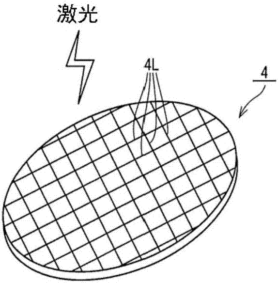
technical field [0001] The present invention relates to a dicing die-bonding film and a method for manufacturing a semiconductor device. Background technique [0002] Conventionally, dicing die-bonding films are sometimes used in the manufacture of semiconductor devices. The dicing die-bonding film is obtained by providing the die-bonding film on a dicing sheet so that it can be peeled off. In the manufacture of a semiconductor device, a semiconductor wafer is held on a die-bonding film for dicing the die-bonding film, and the semiconductor wafer is diced to form individual chips. Then, the chip is peeled from the dicing sheet together with the die-bonding film, and is fixed to adherends such as a lead frame through the die-bonding film. [0003] When using a dicing die-bonding film in which a die-bonding film is laminated on a dicing sheet and dicing a semiconductor wafer while being held by the die-bonding film, it is necessary to cut the die-bonding film and the semicon...

Claims


Application Information

Patent Timeline
Patent Type & Authority Applications(China)
IPC IPC(8): C09J7/02C09J133/00C09J163/00C09J175/14C08G18/62C09J11/08C09J11/04H01L21/683C08F220/18C08F8/30
CPCC08F8/30C08F220/18C08G18/62C08L2205/025C09J11/04C09J11/08C09J133/00C09J163/00C09J175/14C09J2301/208C09J2301/312C09J2423/046C09J2433/00C09J2463/00C09J2475/00H01L21/6836H01L2221/68336C08L63/00C08L61/06C08K7/26C08L33/00C08F220/281
Inventor 大西谦司宍户雄一郎木村雄大福井章洋杉村敏正
Owner NITTO DENKO CORP
Learn More