
Preparation method of semiconductor nanowire array with optimal photoelectric efficiency

A nanowire array and semiconductor technology, which is applied in semiconductor/solid-state device manufacturing, semiconductor devices, nanotechnology for materials and surface science, etc. It can solve the difficulty of optimizing crystal quality, difficult control of array structure, and harsh measurement conditions and other problems, to achieve the effect of efficient collection, high preparation cost, and large consumption of materials

Inactive Publication Date: 2017-10-13
SHANGHAI INST OF TECHNICAL PHYSICS - CHINESE ACAD OF SCI
View PDF6 Cites 3 Cited by
  • Summary
  • Abstract
  • Description
  • Claims
  • Application Information

AI Technical Summary

Problems solved by technology

However, up to now, there is still a lack of a method for preparing semiconductor nanowire arrays that is optimized at both the electrical and optical levels. Although the advantages of using catalytic molecular beam epitaxy to grow nanowire arrays are huge, the crystal quality cannot be guaranteed. Optimization is not easy, and the ideal array structure is not easy to control
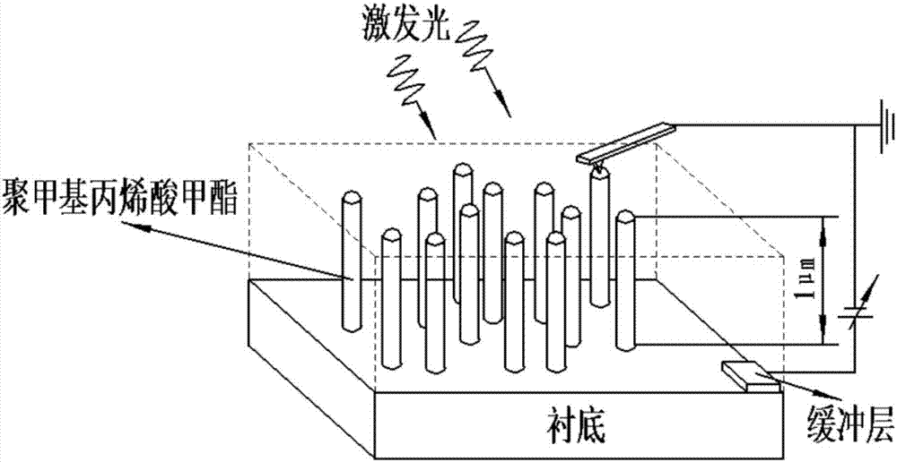
[0006] In addition, the current evaluation methods for the performance of nanowire materials mainly include the analysis of the lattice structure of nanowires by high-resolution electron microscopy and the analysis of optical quality and light absorption characteristics by spectroscopic methods. On the one hand, these methods are complicated in sample preparation and harsh in measurement conditions; On the one hand, they are all separate measurements of the electronic and optical aspects of nanowires, and there is currently a lack of an efficient, direct measurement and evaluation method for the optoelectronic properties of vertical nanowires

Method used


Image

  • Preparation method of semiconductor nanowire array with optimal photoelectric efficiency
  • Preparation method of semiconductor nanowire array with optimal photoelectric efficiency
  • Preparation method of semiconductor nanowire array with optimal photoelectric efficiency

Examples


Embodiment 1

[0020] In this embodiment, a gallium arsenide nanowire array is prepared by using the preparation method provided by the present invention, and the specific steps are as follows:

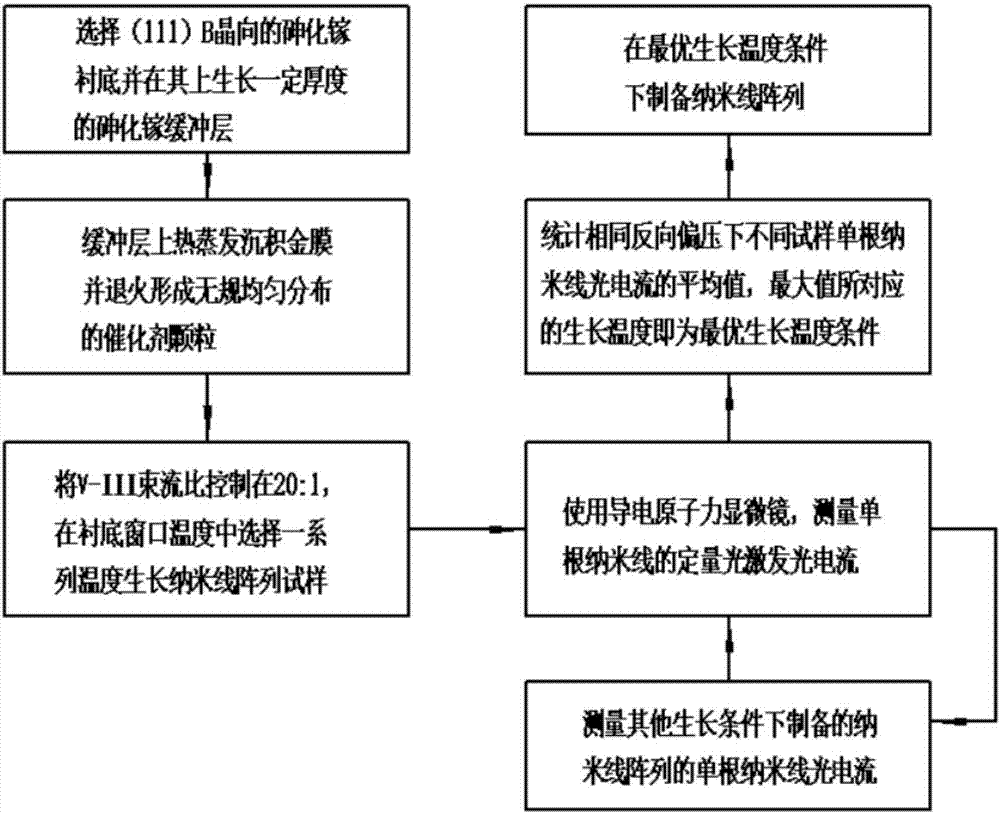
[0021] The preparation process of the semiconductor nanowire array with optimal photoelectric efficiency of the present invention is as follows: figure 1 shown.

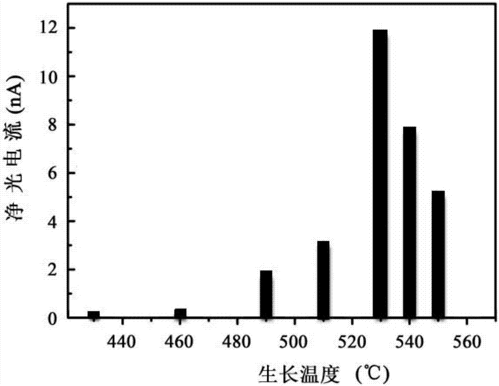
[0022] Firstly, a gallium arsenide substrate with (111) B crystal orientation is selected, the substrate is degassed and deoxidized, and then a 200 nm thick gallium arsenide buffer layer is grown in a molecular beam epitaxy system, and then the gold source is heated by vacuum Heat the furnace to 1000 degrees Celsius, thermally evaporate and deposit a 10-nanometer thick gold film on the buffer layer, and anneal at a substrate temperature of 550 degrees Celsius for 5 minutes to shrink the gold film to form catalyst particles that are randomly and uniformly distributed, and finally use molecular beam epitaxy , the V / III beam ratio is control...

Embodiment 2

[0028]In this example, the preparation method provided by the present invention is used to prepare an indium gallium arsenide nanowire array, wherein the content of the indium component is 30%, and the content of the gallium component is 70%. The preparation of the nanowire array and its photoelectric performance The evaluation process is the same as in Example 1, but the specific parameters are different.

[0029] The substrate window temperature used for growing the nanowire array by molecular beam epitaxy is 406-526 degrees Celsius, and the nanowire array is grown at 406, 436, 466, 486, 506, 516 and 526 degrees Celsius, respectively.

[0030] When using a conductive atomic force microscope to measure the photocurrent-bias curve of a single nanowire in a vertical nanowire array, an excitation light source with a wavelength of 980 nm and a power of 2 mW is used.

[0031] When evaluating the optoelectronic properties of nanowire arrays under different growth conditions, the re...

Embodiment 3

[0033] In this example, an indium arsenide nanowire array is prepared by using the preparation method provided by the present invention. The preparation process of the nanowire array and its photoelectric performance evaluation are the same as those in Example 1, but the specific parameters are different.

[0034] The substrate window temperature used for growing the nanowire array by molecular beam epitaxy is 350-470 degrees Celsius, and the nanowire array is grown at 350, 380, 410, 430, 450, 460 and 470 degrees Celsius, respectively.

[0035] When using a conductive atomic force microscope to measure the photocurrent-bias curve of a single nanowire in a vertical nanowire array, an excitation light source with a wavelength of 2.8 microns and a power of 10 mW is used.

[0036] When evaluating the optoelectronic properties of nanowire arrays under different growth conditions, the reverse bias condition used was 1 volt.


PUM

PropertyMeasurementUnit
Thicknessaaaaaaaaaa

Abstract

The invention discloses a method for preparing a semiconductor nanowire array with optimal photoelectric performance. The method first deposits a gold film by thermal evaporation and anneals to form random and uniformly distributed catalyst particles, and then according to the prepared III-V nanowire material system, select the optimal V / III beam current ratio, grow a series of nanowire array samples at different substrate temperatures, and then use a conductive atomic force microscope to perform statistical evaluation of the vertical photoelectric properties of a single nanowire, and finally The optimal preparation conditions were determined according to the average optoelectronic properties of single nanowires. This method is suitable for catalytic molecular beam epitaxy to grow III-V nanowire arrays such as gallium arsenide, and uses a direct, fast and simple method to evaluate and determine the optimal growth conditions of nanowire arrays through metal catalysis, and then prepares a arrays of semiconducting nanowires with optimal optoelectronic efficiency, and thus, the method is of great interest for the fabrication of high-efficiency solar cells and ultrasensitive photodetectors.

Description

technical field [0001] The invention relates to a method for preparing a semiconductor material with a low-dimensional structure, in particular to a method for preparing a semiconductor nanowire array with optimal photoelectric efficiency. Background technique [0002] Semiconductor vertical nanowire arrays are beneficial for high-efficiency photoelectric conversion both electronically and optically. First of all, nanowires are natural one-dimensional light-wave antennas, coupled with the conduction-resonance mode induced by the array structure, forming a collective "optical trap" effect, making vertical nanowire arrays easier to realize than bulk materials and other semiconductor low-dimensional structures. Light absorption; at the same time, the one-dimensional structure is also more conducive to the efficient collection of photogenerated carriers. These advantages make semiconducting vertical nanowire arrays increasingly promising for applications in high-efficiency sola...

Claims


Application Information

Patent Timeline
IPC IPC(8): H01L31/0693H01L31/18H01L21/02B82Y20/00B82Y30/00
CPCY02E10/544H01L31/0693B82Y20/00B82Y30/00H01L21/02395H01L21/02463H01L21/02546H01L21/02603H01L21/02631H01L21/02658H01L31/184
Inventor 夏辉童中英李天信陈平平卢振宇张健姚晓梅张旭涛唐舟
Owner SHANGHAI INST OF TECHNICAL PHYSICS - CHINESE ACAD OF SCI
Learn More