Supercharge Your Innovation With Domain-Expert AI Agents!

Chip passivation layer and method for forming chip passivation layer

A passivation layer and chip technology, used in semiconductor/solid-state device parts, semiconductor devices, electrical components, etc., can solve problems such as shedding, internal stress changes, and device failures.

Active Publication Date: 2019-06-28
SHANGHAI HUAHONG GRACE SEMICON MFG CORP
View PDF4 Cites 0 Cited by
  • Summary
  • Abstract
  • Description
  • Claims
  • Application Information

AI Technical Summary

Problems solved by technology

During the preparation process of integrated circuits, such as deposition, polishing, photolithography, etc., there will be temperature changes, which will cause the side walls of the metal bumps and the passivation layer on the chip surface to squeeze each other, and the internal stress will change, thereby forming pinholes, Defects such as cracks or shedding cause deformation inside the chip and short circuit or open circuit of interconnecting wires, resulting in device failure
[0004] Therefore, it is necessary to develop a passivation layer of a chip and a method for forming a passivation layer of a chip to solve the problem that the passivation layer in the prior art has pinholes or crack defects

Method used


Image

  • Chip passivation layer and method for forming chip passivation layer
  • Chip passivation layer and method for forming chip passivation layer
  • Chip passivation layer and method for forming chip passivation layer

Examples


Embodiment Construction

[0033] The specific implementations of the passivation layer of the chip and the method for forming the passivation layer of the chip provided by the present invention will be described in more detail below with reference to schematic diagrams. Advantages and features of the present invention will be apparent from the following description and claims. It should be noted that all the drawings are in a very simplified form and use imprecise scales, and are only used to facilitate and clearly assist the purpose of illustrating the embodiments of the present invention.

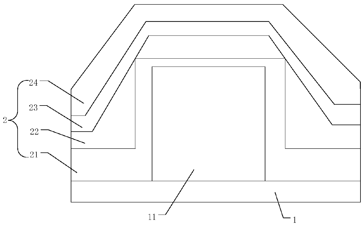
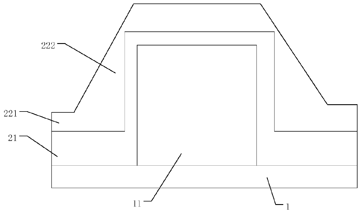
[0034] refer to figure 1 , which is a schematic diagram of the passivation layer of the chip provided by the embodiment, such as figure 1 As shown, the passivation layer 2 includes a first layer 21, a second layer 22, a third layer 23 and a fourth layer 24, and the first layer 21, the second layer 22, the third layer 23 and the fourth layer 24 are sequentially overlapped to cover the chip 1; metal bumps 11 are f...


PUM


Abstract

The invention provides a passivation layer of a chip and a method of forming the passivation layer of the chip. The passivation layer comprises a first chip, a second chip, a third chip, and a fourth layer, which are sequentially superposed together to wrap the chip. The chip is provided with a metal protrusion. The first layer is used to cover the chip and the metal protrusion. The second layer is used to cover the first layer, and the second layer comprises a flat part and a protruding part. An acute angle is formed between the side wall of the protruding part and the side wall of the metal protrusion. The side wall of the protruding part and the side wall of the metal protrusion are used to form a slope, and extrusion between the side wall of the metal protruding block and the passivation layer of the surface of the chip is reduced. The passivation layer of the chip and the method of forming the passivation layer of the chip are advantageous in that stress between the side wall of the metal protruding block and the passivation layer of the surface of the chip is reduced effectively, and the possibilities of the occurrence of the pinholes and the cracks of the passivation layer are reduced, and therefore the yield of the chip is improved, and the service lifetime of the chip is prolonged.

Description

technical field [0001] The invention relates to the field of integrated circuit manufacturing, in particular to a chip passivation layer and a method for forming the chip passivation layer. Background technique [0002] For high-performance and high-reliability integrated circuits, the passivation of the chip surface has become one of the indispensable process measures. The passivation layer is used for electrical isolation between devices and wiring, and to isolate the device from the surrounding environment, so as to enhance the resistance of the device to external ion contamination, protect the internal interconnection of the device and prevent mechanical and chemical damage. [0003] The type and structure of the passivation layer have a great influence on the stress formed inside the interconnection and the speed of stress release. The passivation layer of the existing chip includes an oxide layer and a nitride layer. When depositing an oxide layer and a nitride layer,...

Claims


Application Information

Patent Timeline
Patent Type & Authority Patents(China)
IPC IPC(8): H01L21/56H01L23/31H01L23/29
Inventor 蒙飞
Owner SHANGHAI HUAHONG GRACE SEMICON MFG CORP
Features
  • R&D
  • Intellectual Property
  • Life Sciences
  • Materials
  • Tech Scout
  • Unparalleled Data Quality
  • Higher Quality Content
  • 60% Fewer Hallucinations
Learn More