Eureka AIR delivers breakthrough ideas for toughest innovation challenges, trusted by R&D personnel around the world.

A method for preparing a double-layer silicon nitride film on a semiconductor substrate

A double-layer silicon nitride and semiconductor technology, applied in the field of solar cells, can solve the problems of poor anti-reflection and passivation effect of single-layer silicon nitride film, large interface difference between the bottom film and top film, and increasing the proportion of reworked sheets. Achieve the effect of enhancing passivation and anti-reflection effects, improving appearance, and eliminating interface differences

Active Publication Date: 2021-01-01
HANWHA SOLARONE QIDONG
View PDF5 Cites 0 Cited by
  • Summary
  • Abstract
  • Description
  • Claims
  • Application Information

AI Technical Summary

Problems solved by technology

However, the anti-reflection and passivation effects of the single-layer silicon nitride film are poor, and the double-layer silicon nitride film in the prior art is due to the NH between the two layers of film. 3 / SiH 4 The large difference in the ratio leads to a large interface difference between the bottom film and the top film, which increases the proportion of reworked pieces and reduces the output

Method used


Image

  • A method for preparing a double-layer silicon nitride film on a semiconductor substrate
  • A method for preparing a double-layer silicon nitride film on a semiconductor substrate
  • A method for preparing a double-layer silicon nitride film on a semiconductor substrate

Examples


Embodiment 1

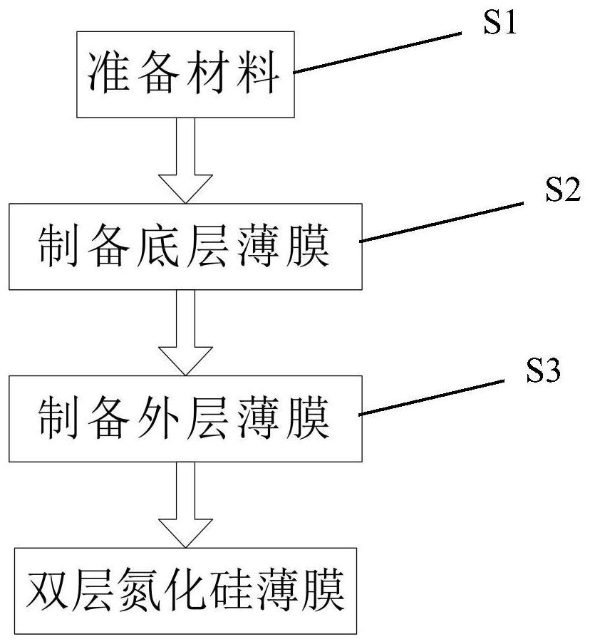
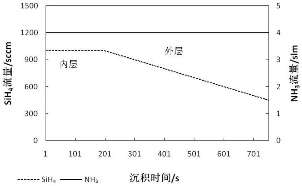
[0026] refer to Figures 1 to 2 , a method for preparing a double-layer silicon nitride film on a semiconductor substrate in this embodiment, comprising the following steps:

[0027] Step S1: Prepare materials

[0028] Prepare clean silicon wafers.

[0029] Step S2: Prepare the underlying film

[0030] Put the silicon wafer into the deposition equipment, and pass the reaction gas SiH into the deposition chamber 4 and NH 3 And by setting the first deposition condition, the underlying silicon nitride film is deposited on the silicon wafer.

[0031] The first deposition condition is: deposition power is 6000W, pressure is 1500mTorr, time is 200s, NH 3 flow rate of 4 slm, SiH 4 The flow rate is 1000sccm. Control NH 3 and SiH 4 The flow rate is fixed and a certain thickness of the underlying film is deposited to ensure the passivation effect of the underlying film.

[0032] Step S3: Prepare the outer film

[0033] Continue to feed reaction gas SiH in the deposition chamb...

Embodiment 2

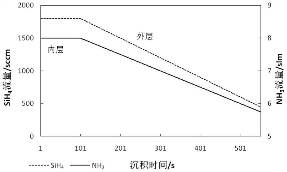
[0036] refer to figure 1 with image 3 , a method for preparing a double-layer silicon nitride film on a semiconductor substrate in this embodiment, comprising the following steps:

[0037] Step S1: Prepare materials

[0038] Prepare clean silicon wafers.

[0039] Step S2: Prepare the underlying film

[0040] Put the silicon wafer into the deposition equipment, and pass the reaction gas SiH into the deposition chamber 4 and NH 3 And by setting the first deposition condition, the underlying silicon nitride film is deposited on the silicon wafer.

[0041] The first deposition condition is: deposition power is 8000W, pressure is 2000mTorr, time is 100s, NH 3 flow rate of 8 slm, SiH 4 The flow rate is 1800sccm. Control reaction gas NH 3 and SiH 4 The flow rate is fixed and a certain thickness of the underlying film is deposited to ensure the passivation effect of the underlying film.

[0042] Step S3: Prepare the outer film

[0043] Continue to feed reaction gas SiH in...

Embodiment 3

[0046] refer to figure 1 with Figure 4 , a method for preparing a double-layer silicon nitride film on a semiconductor substrate in this embodiment, comprising the following steps:

[0047] Step S1: Prepare materials

[0048] Prepare clean silicon wafers.

[0049] Step S2: Prepare the underlying film

[0050] Put the silicon wafer into the deposition equipment, and pass the reaction gas SiH into the deposition chamber 4 and NH 3 And by setting the first deposition condition, the underlying silicon nitride film is deposited on the silicon wafer.

[0051] The first deposition condition is: deposition power is 7000W, pressure is 1700mTorr, time is 100s, NH 3 flow rate of 5 slm, SiH 4 The flow rate is 1000sccm. Control NH 3 and SiH 4 The flow rate is fixed and a certain thickness of the underlying film is deposited to ensure the passivation effect of the underlying film.

[0052] Step S3: Prepare the outer film

[0053] Continue to feed SiH in the deposition chamber a...


PUM


Abstract

The present invention discloses a method for preparation of a dual-layer silicon nitride film on a semiconductor substrate. The method comprises the following steps: (1) material preparation: preparing a clean semiconductor substrate; (2) preparation of base layer film: putting the semiconductor substrate into a deposition device, inletting reaction gas SiH3 and NH3 in a deposition cavity and arranging a first deposition condition, and performing deposition of a base layer silicon nitride film on the semiconductor substrate; and (3) preparation of an external layer film: arranging a second deposition condition to control the gradual reduction of the SIH4 reaction gas and uniform changing of the flow of the NH3 reaction gas, forming an external layer silicon nitride film at the external surface of the base layer silicon nitride film, and finally forming a dual-layer silicon nitride film structure. The method for preparation of the dual-layer silicon nitride film on the semiconductor substrate eliminates the interface difference between the base layer film and the external layer film in a traditional dual-layer silicon nitride film so as to improve the light absorption, improve the passivation and antireflection effect and improve the efficiency of a solar battery.

Description

technical field [0001] The invention relates to the technical field of solar cells, in particular to a method for preparing a double-layer silicon nitride film on a semiconductor substrate. Background technique [0002] With the continuous development of photovoltaic technology, solar cell products, which are semiconductor devices that convert solar energy into electrical energy, have been rapidly developed. The PECVD (Plasma Enhanced Chemical Vapor Deposition) process is an important link in the preparation of silicon solar cells. It mainly has the following advantages: anti-reflection effect; passivation of the surface of the silicon wafer to reduce the surface recombination rate; to the passivation effect. However, the anti-reflection and passivation effects of the single-layer silicon nitride film are poor, and the double-layer silicon nitride film in the prior art is due to the NH between the two layers of film. 3 / SiH 4 The large ratio difference results in a large ...

Claims


Application Information

Patent Timeline
Patent Type & Authority Patents(China)
IPC IPC(8): H01L21/02
CPCH01L21/02365H01L21/02521
Inventor 张欣何胜赵福祥金起弘
Owner HANWHA SOLARONE QIDONG
Why Eureka
Eureka Blog
Learn More