A dielectric silicon photonic crystal fiber and its manufacturing method

A technology of crystal fiber and manufacturing method, which is applied to cladding fiber, optical waveguide and light guide, etc., to achieve the effects of simple equipment, fast preparation speed and saving production cost

Active Publication Date: 2019-09-27
NORTHEASTERN UNIV LIAONING
View PDF4 Cites 0 Cited by
  • Summary
  • Abstract
  • Description
  • Claims
  • Application Information

AI Technical Summary

Problems solved by technology

[0006] The invention provides a dielectric silicon photonic crystal fiber and its manufacturing method, which solves the problem that the current dielectric silicon nanoparticle structure can only be produced on a planar structure through expensive nano-processing equipment, combining dielectric silicon nanoparticles, optical UV glue and Quartz capillary

Method used


Image

  • A dielectric silicon photonic crystal fiber and its manufacturing method

Examples


Embodiment Construction

[0020] The essential features and remarkable progress of the present invention will be clarified below through specific embodiments.

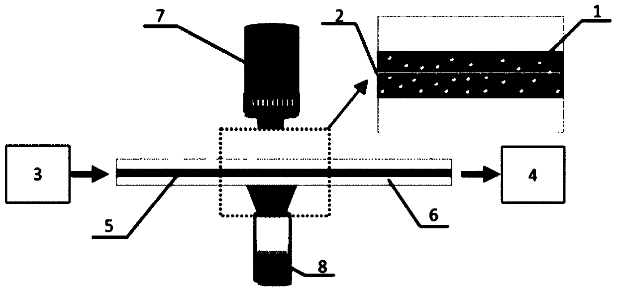
[0021] A method for manufacturing dielectric silicon photonic crystal optical fibers. Compared with traditional photonic crystal optical fiber preparation processes, the UV glue itself is liquid, transparent and easy to be doped to achieve uniform distribution of dielectric silicon nanoparticles in it, forming and Preparation of optical fiber with three-dimensional photonic crystal structure, dielectric silicon nanoparticle 1, micron optical fiber 2, broad-spectrum laser 3, spectrum analyzer 4, optical UV glue 5, quartz capillary 6, microscope 7, and ultraviolet light curing device 8. The specific implementation method is to inject the optical UV glue 5 containing the medium silicon nanoparticles 1 into the quartz capillary 6 by using a micro-injector, and use the ultrasonic oscillation technology to evenly disperse and suspend the medium silico...


PUM

PropertyMeasurementUnit
diameteraaaaaaaaaa
wavelengthaaaaaaaaaa

Abstract

The invention discloses a dielectric silicon photonic crystal fiber and a manufacture method thereof. The dielectric silicon photonic crystal fiber comprises dielectric silicon nano-particles, a micron optical fiber, a wide-spectrum laser, a spectrum analyzer, optical UV glue, a quartz capillary tube, a microscope and an ultraviolet light solidifying device. According to the dielectric silicon photonic crystal fiber and the manufacture method thereof of the invention, the dielectric silicon nano-particles are uniformly dispersed in the optical UV glue, the change of a transmission spectrum is monitored in real time by means of the wide-spectrum laser and the spectrum analyzer; the ultraviolet light solidifying device is utilized to solidify the optical UV glue, so that a solid photonic crystal structure is obtained; and the formation process of the photonic crystal fiber structure is observed through using the microscope. Since the dielectric silicon nano-particles have local optical field enhancement and zero backscattering features, with the dielectric silicon photonic crystal fiber obtained through using the manufacture method of the invention adopted, the research and development of novel biochemical sensors and photonic devices can be facilitated.

Description

technical field [0001] Based on the local light field enhancement and zero backscattering characteristics of dielectric silicon nanoparticles, the invention provides a dielectric silicon photonic crystal fiber and a manufacturing method thereof. Background technique [0002] Photonic crystal fiber, also known as microstructured fiber, was first proposed by Russell in 1992, and its light guiding performance was theoretically verified by Birks in 1995, and it was successfully prepared for the first time in 1999. It can realize the spatial modulation of optical signals through subwavelength periodic microstructures. In recent years, it has attracted extensive attention and developed rapidly in the fields of nonlinear optics, laser-induced transmission, biomedical imaging, optical sensing, and quantum optical devices. In the future, this technology will open up more research directions in other scientific research and engineering fields, and it is urgent to expand its applicatio...

Claims


Application Information

Patent Timeline
Patent Type & Authority Patents(China)
IPC IPC(8): G02B6/02
Inventor 李晋董书琳胡海峰
Owner NORTHEASTERN UNIV LIAONING
Why Eureka
Try Eureka