Silicon carbide VDMOS device
A technology of silicon carbide and devices, which is applied in the direction of semiconductor devices, electrical components, circuits, etc., can solve the problems of reduced forward current capability of devices, lower peak electric field of gate oxide layer, etc., to reduce electric field peak value, improve electric field uniformity, increase reliability effect
- Summary
- Abstract
- Description
- Claims
- Application Information
AI Technical Summary
Problems solved by technology
Method used
Image


Examples
Embodiment 1
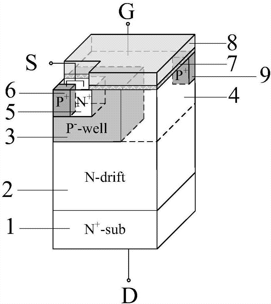
[0017] Such as figure 1 As shown, this example is the case where the P-type implantation region 9 is any P-type implantation, including the N+ substrate 1, the N-type epitaxial layer, and the gate structure. Wherein, the N epitaxial layer is located on the N+ substrate 1 , and the gate structure is located on the N epitaxial layer.
[0018] The gate structure covers the surface except the source, and the gate structure includes a gate dielectric layer 7 and polysilicon 8 thereon, and the polysilicon surface leads out to the gate; the upper part of the N epitaxial layer forms horizontal and vertical segmented P-type well regions 3, a JFET region 4 is formed between the P-type well regions 3, an independent N+ source region 5 and a P+ body contact region 6 are formed on the upper part of the P-type well region, wherein the N+ source region 5 surrounds the P+ body contact region 6, The common terminal of the N+ source region 5 and the P+ body contact region 6 is the source; the ...
Embodiment 2
[0023] Such as figure 2 As shown, the structure of this example is basically the same as that of Example 1, except that the P-type implanted region 9 and the P+ body contact region 6 have the same junction depth and doping concentration.
[0024] Compared with Example 1, this example can save a mask in the process, reduce one ion implantation, and reduce the cost.
Embodiment 3
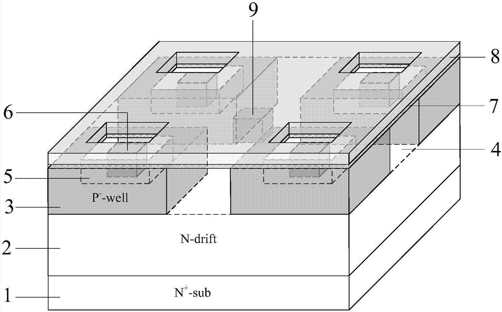
[0026] Such as Figure 5 As shown, the structure of this example is basically the same as that of Example 1, except that the P-type implant region 9 and the P-type well region 3 have the same junction depth and doping concentration.
[0027] Compared with Example 1, this example can save a mask in the process, reduce one ion implantation, and reduce the cost. Compared with Example 2, the junction depth of the P-type implanted region 9 in this example is deeper, which can more significantly reduce the peak value of the electric field of the gate oxide layer and improve the withstand voltage of the device.
PUM
 Abstract
Description
Claims
Application Information
 - R&D
- Intellectual Property
- Life Sciences
- Materials
- Tech Scout
- Unparalleled Data Quality
- Higher Quality Content
- 60% Fewer Hallucinations
Browse by: Latest US Patents, China's latest patents, Technical Efficacy Thesaurus, Application Domain, Technology Topic, Popular Technical Reports.
© 2025 PatSnap. All rights reserved.Legal|Privacy policy|Modern Slavery Act Transparency Statement|Sitemap|About US| Contact US: help@patsnap.com