Low-temperature epitaxy preparation method of germanium-silicon film with high germanium content

A kind of content, germanium silicon technology, applied in the field of optimization of germanium silicon thin film growth conditions, can solve the problems of complex operation, high cost, waste of time, etc., and achieve the effect of simple operation, low cost and clear interface

Active Publication Date: 2017-11-03
NANJING UNIV
View PDF3 Cites 2 Cited by
  • Summary
  • Abstract
  • Description
  • Claims
  • Application Information

AI Technical Summary

Problems solved by technology

This method is complicated to operate and needs to constantly change the ratio of germanium to silicon, which is a waste of time and high cost

Method used


Image

  • Low-temperature epitaxy preparation method of germanium-silicon film with high germanium content
  • Low-temperature epitaxy preparation method of germanium-silicon film with high germanium content
  • Low-temperature epitaxy preparation method of germanium-silicon film with high germanium content

Examples


Embodiment Construction

[0025] The present invention will be described in further detail below in conjunction with the accompanying drawings and specific embodiments.

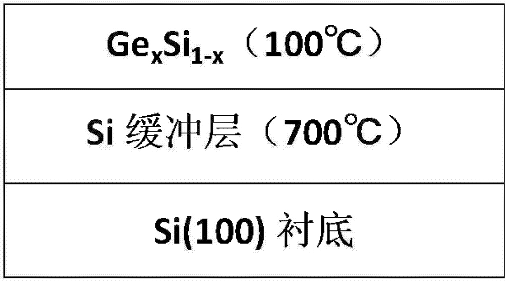
[0026] The invention provides a silicon germanium (Ge silicon) with adjustable lattice constant grown on a silicon chip by molecular beam epitaxy at low temperature. x Si 1-x ) film preparation method. figure 1 It is silicon germanium (Ge x Si 1-x ) Schematic diagram of the structure of the thin film, the specific preparation method is as follows:

[0027] Through solid-state source molecular beam epitaxy, the (100) crystal plane silicon substrate is first deoxidized, that is, the oxide on the surface is removed. Keeping the substrate rotating at a rotation speed of 10 rpm, the substrate heater was raised to 1350° C. for 10 minutes.

[0028] Then grow a 50nm Si buffer layer on the deoxidized Si(100) substrate by molecular beam epitaxy. The growth temperature was 700°C, and the growth rate was The Si source furnace used in this...


PUM


Abstract

The invention discloses a low-temperature epitaxy preparation method of a germanium-silicon film with high germanium content. The low-temperature epitaxy preparation method comprises the following specific steps: (1) providing a silicon substrate with a (100) crystal face; (2) carrying out deoxidation on the silicon substrate at the temperature of 1350 DEG C, wherein the deoxidation lasts for 10 minutes; (3) through a molecular beam epitaxy method, growing a silicon buffer layer with the thickness of 20 to 50 nm on the silicon substrate after deoxidation, wherein the growth temperature is 700 DEG C; and (4) cooling the silicon buffer layer to a growth temperature which is below 300 DEG C, then growing GexSi1-x alloy, and adjusting the content of Ge, namely an x value, by changing the growth rates of Ge and Si. According to the preparation method, the high-quality germanium-silicon (GexSi1-x) film material with adjustable lattice constants can be directly grown on the silicon wafer at low temperature, and the content of germanium at most can reach 83%. The method does not need to adopt a layer-by-layer growth pattern for improving the content of germanium layer by layer, so that the method is simpler in operation and lower in cost.

Description

technical field [0001] The present invention relates to a method for directly growing germanium-silicon alloy thin films on silicon wafers, more specifically, it relates to the optimization of growth conditions for direct epitaxial germanium-silicon thin films with high germanium content (germanium content greater than 50%) on silicon wafers, Including the treatment of the substrate, the growth of the buffer layer and the optimization process of the growth temperature of the silicon-germanium alloy. Background technique [0002] Silicon (Si) and germanium (Ge) are the most common semiconductor materials and are also important materials for electronic components. Germanium-silicon alloy with adjustable band gap, adopting standard CMOS technology, can obtain ideal electronic control performance, and has important application value. However, since the lattice mismatch between germanium and silicon is above 4%, it is difficult to obtain high-quality germanium-silicon epitaxial ...

Claims


Application Information

Patent Timeline
Patent Type & Authority Applications(China)
IPC IPC(8): H01L21/02
CPCH01L21/02381H01L21/02532H01L21/02617H01L21/02628
Inventor 芦红叶佳佳
Owner NANJING UNIV
Why Eureka
Try Eureka