Aluminum nitride film growing on silicon substrate and preparation method and application thereof

A growth method and substrate technology, applied in the final product manufacturing, sustainable manufacturing/processing, electrical components, etc., can solve the problems of slow growth of a single film, high cost of a single sample, complex equipment and instruments, etc., to shorten the nucleation. The effect of excellent temporal, electrical and optical properties and high crystal quality

Active Publication Date: 2015-03-04
广州市艾佛光通科技有限公司
View PDF1 Cites 2 Cited by
  • Summary
  • Abstract
  • Description
  • Claims
  • Application Information

AI Technical Summary

Problems solved by technology

However, most of the preparation methods require the substrate to be heated to a higher temperature, but the higher temperature may cause damage to the substrate material, which is a major problem in the preparation of AlN thin films
Moreover, to meet the requirements of growing high-quality AlN crystals, complex equipment and instruments are required, which are expensive, and the growth rate of a single film is slow, and the cost of a single sample is too high

Method used


Image

  • Aluminum nitride film growing on silicon substrate and preparation method and application thereof
  • Aluminum nitride film growing on silicon substrate and preparation method and application thereof
  • Aluminum nitride film growing on silicon substrate and preparation method and application thereof

Examples


Embodiment 1

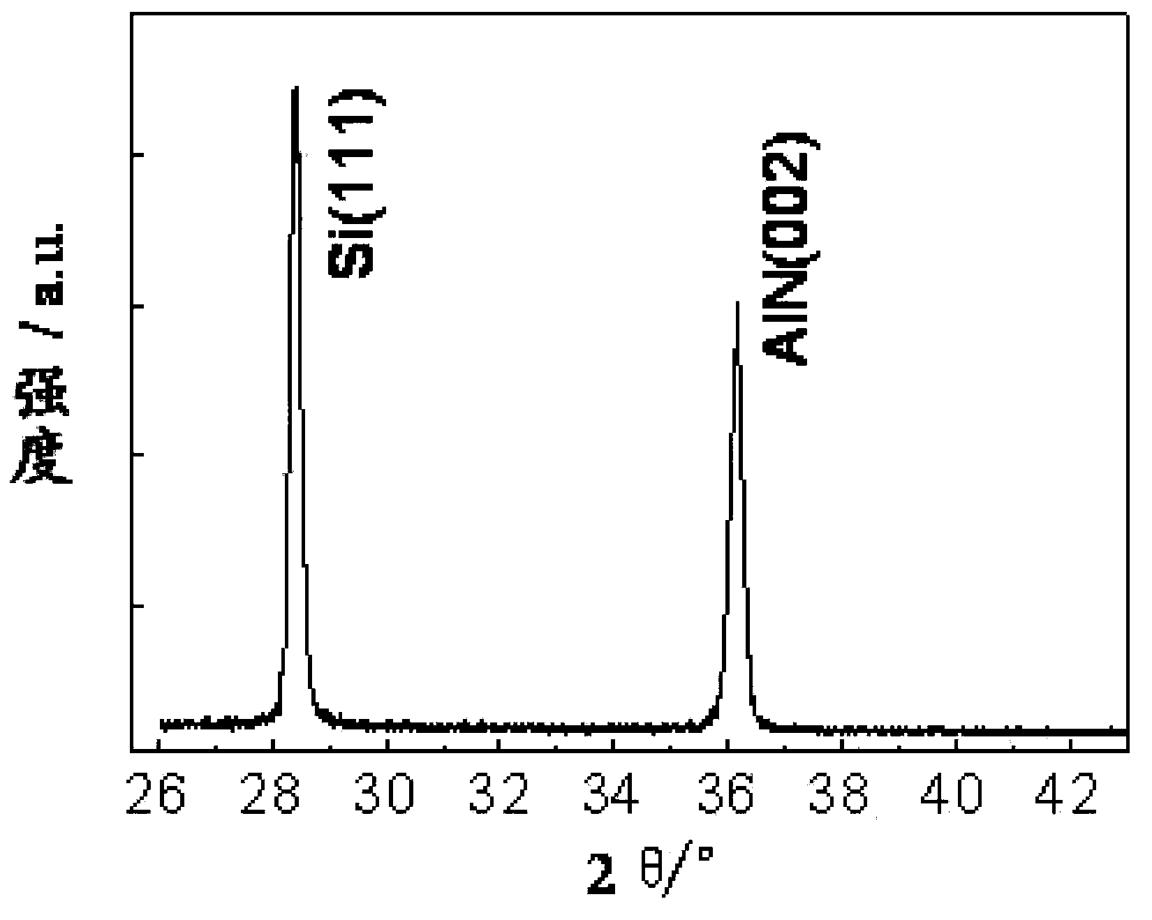
[0032] Please refer to figure 1 The AlN film grown on the Si substrate of the present invention includes a Si substrate layer 11 and an AlN film layer 12 grown on the Si substrate layer 11. The AlN thin film layer 12 is a single crystal thin film layer or a polycrystalline thin film layer.

[0033] The AlN film grown on the Si substrate is prepared by the following method:

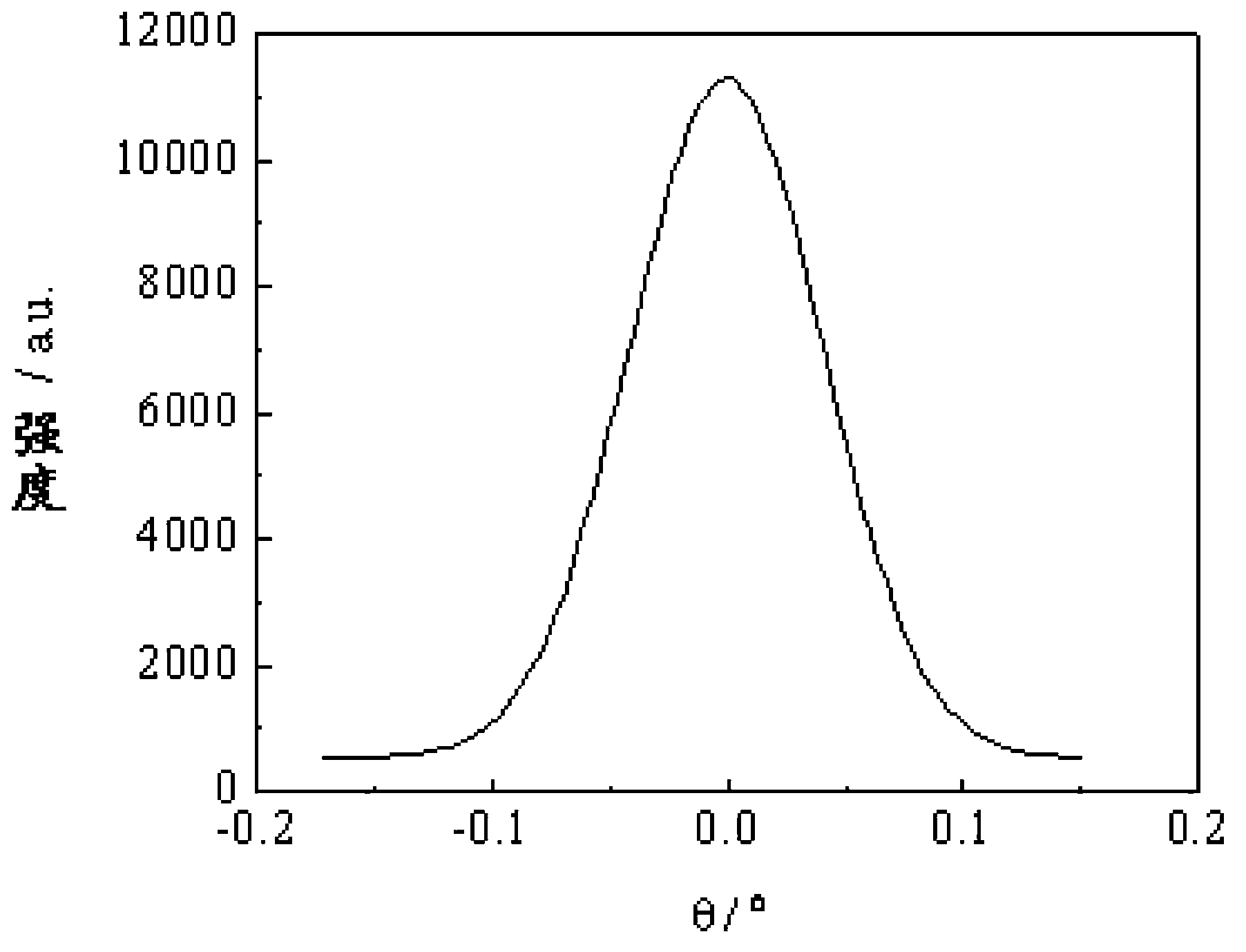
[0034] (1) The choice of substrate and crystal orientation: select Si substrate, and select the (111) crystal plane of Si substrate.

[0035] (2) Using molecular beam epitaxial growth method to grow Al buffer layer on Si substrate, the process conditions are:

[0036] The substrate temperature is 500-600℃, and the vacuum degree is 10 -10 Above Torr, the growth rate is 0.6nm / min, and the thickness of the grown Al buffer layer is 3-5nm. The growth is detected and controlled by RHEED.

[0037] (3) Nitriding the Al buffer layer by passing nitrogen plasma.

[0038] (4) Using pulsed laser deposition growth method to grow ...

Embodiment 2

[0042] This embodiment is modified on the basis of embodiment 1, and the difference is that: before the AlN buffer layer is grown, the substrate is subjected to the pretreatment steps of surface polishing, cleaning, and annealing in sequence. The specific method is as follows:

[0043] Surface polishing treatment: polishing the surface of the Si substrate with diamond slurry, observing that the surface of the substrate is free of scratches with an optical microscope, and then polishing the substrate by the prior art chemical mechanical polishing method.

[0044] Cleaning: Put the card slot containing the Si film into the cleaned square bottle, add deionized water and the prepared acetone until the solution is completely immersed in the Si film, ultrasound for 5-10 minutes; put the square bottle in the ultrasonic tank , Add deionized water until the water level is slightly lower than the square bottle, perform ultrasonic cleaning for 5-10 minutes, the ultrasonic power is 60-80 watts;...

Embodiment 3

[0050] Example 3 Application of AlN thin film grown on Si substrate of the present invention in LED devices

[0051] Please refer to Figure 5 , The method of applying the AlN film obtained in Example 2 to LED devices includes epitaxially growing a high-quality AlN film on the Si (111) crystal plane, and after forming the AlN film 10, sequentially growing high-quality U-GaN film layers 11. n-type silicon-doped GaN epitaxial layer 12. In x Ga 1-x N multiple quantum well layer 13, p-type magnesium-doped GaN layer 14, as follows:

[0052] A high-quality U-GaN thin film layer 11 is grown on the AlN thin film 10; then an n-type silicon-doped GaN epitaxial layer 12 is grown on the U-GaN thin film layer 11, with a thickness of about 5 μm and a carrier concentration of 1 ×10 19 cm - 3 . Then grow In x Ga 1-x N multiple quantum well layer 13, the thickness is about 112 nm, the number of periods is 7, where In x Ga 1-x The N-well layer is 3 nm, the barrier layer is 13 nm, and 016 cm - 3 . ...


PUM

PropertyMeasurementUnit
thicknessaaaaaaaaaa
thicknessaaaaaaaaaa
thicknessaaaaaaaaaa

Abstract

The invention discloses an aluminum nitride film growing on a silicon substrate and a preparation method and the application thereof. The aluminum nitride film is obtained by the following preparation method: adopting the silicon substrate, selecting the (111) crystal face of the silicon substrate as crystal orientation, growing an aluminum buffer layer on the (111) crystal face of the silicon and then growing an aluminum nitride film in epitaxial growth mode. The silicon is adopted as the substrate, simultaneously a pulse laser deposition growth method is adopted to grow the aluminum nitride film on the Si (111) substrate, the aluminum nitride film crystal grows in preferred orientation to obtain low lattice mismatch degree between the substrate and the aluminum nitride, quality of the aluminum nitride crystal is greatly improved, and the aluminum nitride film is suitable for being applied to photoelectric detectors and light-emitting diode (LED) devices.

Description

Technical field [0001] The invention relates to the field of AlN thin films, in particular to an AlN thin film grown on a Si substrate and a preparation method and application thereof. Background technique [0002] AlN is a group IIIA compound, which generally exists in the wurtzite structure in the hexagonal crystal system. It has many excellent properties, such as high thermal conductivity, low thermal expansion coefficient, high electrical insulation properties, high dielectric breakdown strength, and excellent The mechanical strength, excellent chemical stability and low toxicity, good optical properties, etc. Because AlN has many excellent properties, wide band gap, strong polarization, and a band gap of 6.2 eV, it can be used in machinery, microelectronics, optics, and electronic components, surface acoustic wave device manufacturing, high-frequency broadband communication and power Semiconductor devices and other fields have broad application prospects. [0003] At present...

Claims


Application Information

Patent Timeline
Patent Type & Authority Patents(China)
IPC IPC(8): H01L33/12H01L31/0352H01L31/18
CPCY02P70/50
Inventor 李国强
Owner 广州市艾佛光通科技有限公司
Why Eureka
Try Eureka