
Non-polar doped GaN film grown on LiGaO2 substrate and preparation method thereof

A non-polar, thin-film technology, applied in the field of non-polar doped GaN thin films and their preparation, can solve the problems of reduced carrier radiation recombination efficiency, unstable luminous wavelength, and influence on LED luminous efficiency, etc. The effect of reducing production cost and improving luminous efficiency

Active Publication Date: 2013-04-10
SOUTH CHINA UNIV OF TECH
View PDF1 Cites 3 Cited by
  • Summary
  • Abstract
  • Description
  • Claims
  • Application Information

AI Technical Summary

Problems solved by technology

On the polar plane of GaN, the centroids of the Ga atom assembly and the N atom assembly do not coincide, thereby forming an electric dipole, generating a spontaneous polarization field and a piezoelectric polarization field, and then causing the quantum-confined Stark effect (Quantum-confined Starker Effect, QCSE), which separates electrons and holes, and reduces the radiative recombination efficiency of carriers, which ultimately affects the luminous efficiency of LEDs and causes instability of LED luminous wavelengths.

Method used


Image

  • Non-polar doped GaN film grown on LiGaO2 substrate and preparation method thereof
  • Non-polar doped GaN film grown on LiGaO2 substrate and preparation method thereof
  • Non-polar doped GaN film grown on LiGaO2 substrate and preparation method thereof

Examples


Embodiment 1

[0031] The present invention grows on LiGaO 2A method for preparing a doped GaN thin film on a substrate, comprising the following steps:

[0032] (1) Select the substrate and crystal orientation: use LiGaO 2 The substrate, the crystal orientation is (100) crystal plane deflected to (110) direction by 0.2°.

[0033] (2) Annealing the substrate: Baking the substrate at 900° C. for 3 hours, then air cooling to room temperature.

[0034] (3) Clean the surface of the substrate: LiGaO 2 The substrate was ultrasonically cleaned in deionized water for 5 minutes at room temperature to remove LiGaO 2 The dirt particles on the surface of the substrate are washed with hydrochloric acid, acetone, and ethanol in sequence to remove surface organic matter; the cleaned LiGaO 2 The substrate was blown dry with high-purity dry nitrogen; after that, the LiGaO 2 Put the substrate into a low-temperature molecular beam epitaxy growth chamber, raise the substrate temperature to 850°C under ultr...

Embodiment 2

[0042] The present invention grows on LiGaO 2 The preparation method of the nonpolar doped GaN thin film on the substrate comprises the following steps:

[0043] (1) Select the substrate and crystal orientation: use LiGaO 2 The substrate, the crystal orientation is that the (100) crystal plane is deflected to the (110) direction by 0.5°.

[0044] (2) Annealing the substrate: Baking the substrate at a high temperature of 1000° C. for 5 hours, then air cooling to room temperature.

[0045] (3) Clean the surface of the substrate: LiGaO 2 The substrate was ultrasonically cleaned in deionized water for 10 minutes at room temperature to remove LiGaO 2 The dirt particles on the surface of the substrate are washed with hydrochloric acid, acetone, and ethanol in sequence to remove surface organic matter; the cleaned LiGaO 2 The substrate was blown dry with high-purity dry nitrogen; after that, the LiGaO 2 The substrate is placed in a low-temperature molecular beam epitaxy growth c...

Embodiment 3

[0053] In this embodiment, except the following features, all the other features are the same as in Embodiment 1:

[0054] Step (6) is: using pulsed laser deposition process to grow non-polar n-type doped GaN film with a thickness of 5 μm. The process conditions are: the substrate temperature is 550 ° C, the pulsed laser is used to bombard the GaSi mixed target, and the growth is fed into N plasma, the reaction chamber pressure is 7×10 -5 torr, the RF power is 300W, the laser energy is 180mJ, and the frequency is 30Hz.


PUM

PropertyMeasurementUnit
Thicknessaaaaaaaaaa
Thicknessaaaaaaaaaa
Thicknessaaaaaaaaaa

Abstract

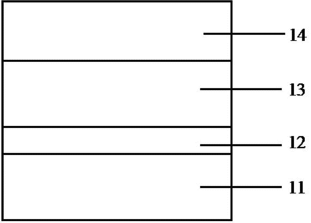
The invention discloses a doped GaN film grown on a LiGaO2 substrate. The doped GaN film comprises the LiGaO2 substrate, a non-polar m-surface GaN buffer layer, a non-polar m-surface GaN epitaxial layer and a non-polar doped GaN film, wherein the non-polar GaN film is a non-polar p-type GaN film or a non-polar n-type GaN film. The invention also discloses a preparation method of the non-polar doped GaN film. Compared with the prior art, the non-polar doped GaN film has the advantages of simple growth process and low preparation cost, and the prepared non-polar doped GaN film is low in defect density, good in crystallization quality and high in electrical property.

Description

technical field [0001] The present invention relates to non-polar doped GaN thin film and preparation method thereof, especially relate to the growth on LiGaO 2 Nonpolar doped GaN film on substrate and its preparation method. Background technique [0002] LED is called the fourth-generation lighting source or green light source. It has the characteristics of energy saving, environmental protection, long life, and small size. It can be widely used in various general lighting, indication, display, decoration, backlight, and urban night scenes. At present, under the background of the increasingly serious problem of global warming, saving energy and reducing greenhouse gas emissions has become an important issue faced by the whole world. A low-carbon economy based on low energy consumption, low pollution, and low emissions will become an important direction of economic development. In the field of lighting, the application of LED light-emitting products is attracting the atten...

Claims


Application Information

Patent Timeline
IPC IPC(8): C30B25/02C30B25/18C30B25/00C30B29/38
Inventor 李国强杨慧
Owner SOUTH CHINA UNIV OF TECH
Learn More