Method for optimizing the channel conductivity of diamond material

A technology of conductive characteristics and optimization methods, which is applied in the direction of circuits, electrical components, semiconductor devices, etc., can solve the problem of low hole concentration, achieve the effect of simple steps, improve performance, and improve channel conductivity

Inactive Publication Date: 2017-11-07
INST OF MICROELECTRONICS CHINESE ACAD OF SCI
View PDF11 Cites 1 Cited by
  • Summary
  • Abstract
  • Description
  • Claims
  • Application Information

AI Technical Summary

Problems solved by technology

[0006] The invention provides a method for optimizing the channel conduction characteristics of diamond materials, which can improve the channel conduction ability of the surface of diamond materials in order to improve the performance of diamond substrate devices in view of the lack of low hole concentration of diamond materials in the prior art

Method used


Image

  • Method for optimizing the channel conductivity of diamond material
  • Method for optimizing the channel conductivity of diamond material
  • Method for optimizing the channel conductivity of diamond material

Examples


Embodiment Construction

[0027] In order to make the purpose, technical solutions and advantages of the embodiments of the present invention clearer, the technical solutions in the embodiments of the present invention will be clearly and completely described below in conjunction with the drawings in the embodiments of the present invention. Obviously, the described embodiments It is only some embodiments of the present invention, but not all embodiments. Based on the embodiments of the present invention, all other embodiments obtained by persons of ordinary skill in the art without making creative efforts belong to the protection scope of the present invention.

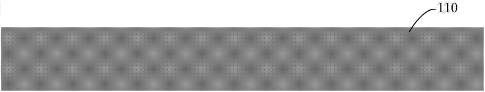
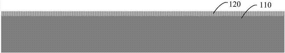
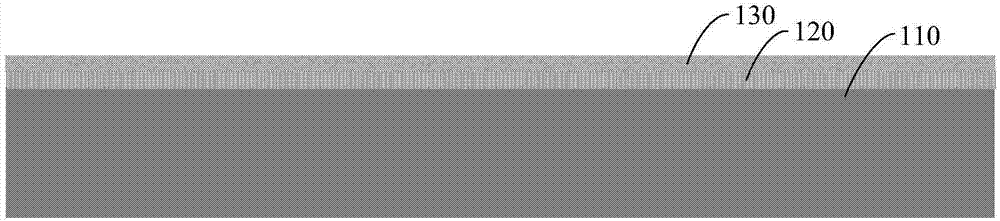
[0028] The invention provides a method for optimizing the conductivity characteristics of a diamond material channel, such as Figure 1a As shown, a diamond substrate 110 is provided. In particular, the diamond substrate can be cleaned, and the cleaning method includes but is not limited to ultrasonic cleaning in acetone solution, followed b...


PUM

PropertyMeasurementUnit
thicknessaaaaaaaaaa
breakdown field strengthaaaaaaaaaa

Abstract

The invention provides a method for optimizing the channel conductivity of a diamond material. The method comprises a first step of providing a diamond substrate; a second step of treating the surface of the diamond substrate with a hydrogen plasma to form a hydrogen plasma treatment layer; a third step of depositing a first oxide layer on the hydrogen plasma treatment layer; a fourth step of depositing a second oxide layer on the first oxide layer and photoetching a gate dielectric layer; a fifth step of growing a source/drain electrode metal on the device formed in the fourth step; and a sixth step of growing a gate electrode metal on the device formed in the fifth step. The method of the invention can improve the channel conductivity of the hydrogen-terminated diamond surface.

Description

technical field [0001] The invention relates to the technical field of microelectronics and nanoelectronic devices, in particular to a method for optimizing the conduction characteristics of a diamond material channel. Background technique [0002] With the shrinking of transistor feature size, due to physical laws such as short channel effects and manufacturing cost constraints, mainstream silicon-based materials and CMOS technology are developing to the 10nm process node and it is difficult to continue to improve. At present, diamond is considered as a new generation of integrated circuit semiconductor material because of its excellent characteristics. Diamond has an ultra-wide band gap (5.7eV), extremely high thermal conductivity (2000w / (m k)), a large breakdown electric field (10MV / cm) and high carriers (electrons and holes) Mobility has wide application prospects in high frequency, high power and optical components. [0003] However, on the one hand, the post-doping p...

Claims


Application Information

Patent Timeline
Patent Type & Authority Applications(China)
IPC IPC(8): H01L29/10H01L29/16H01L29/78H01L21/336
CPCH01L29/1033H01L29/1602H01L29/66045H01L29/78
Inventor 龙世兵董航何启鸣刘明
Owner INST OF MICROELECTRONICS CHINESE ACAD OF SCI
Why Eureka
Try Eureka