SOI LIGBT with controllable collector trough

A collector and collector area technology, applied in circuits, electrical components, semiconductor devices, etc., can solve problems such as serious hot carrier injection, increase process difficulty and cost, affect device stability and reliability, etc., and achieve fast Turn-off speed, enhanced hole injection efficiency, and the effect of eliminating the snapback phenomenon

Active Publication Date: 2017-11-10
UNIV OF ELECTRONICS SCI & TECH OF CHINA +1
View PDF11 Cites 10 Cited by
  • Summary
  • Abstract
  • Description
  • Claims
  • Application Information

AI Technical Summary

Problems solved by technology

This method can eliminate the Snapback effect, but the fabrication of deep grooves will increase the difficulty and cost of the process
In addition, the deep groove is at the collector end, and the hot carrier injection is serious, which will affect the stability and reliability of the device

Method used


Image

  • SOI LIGBT with controllable collector trough
  • SOI LIGBT with controllable collector trough
  • SOI LIGBT with controllable collector trough

Examples


Embodiment 1

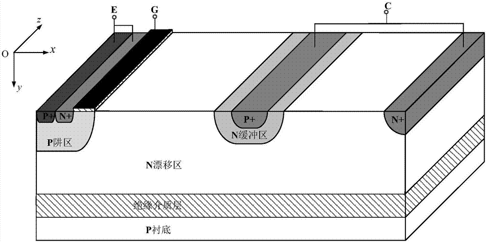
[0023] Such as Figure 4 As shown, the SOI LIGBT with a controllable collector groove in this example includes a bottom-up substrate layer 1, an insulating dielectric layer 2, and an N-type drift region 3; one end of the N-type drift region 3 includes an emitter structure and The gate structure, the other end includes a collector structure and a collector groove structure.

[0024] The emitter structure includes a P well region 4, a P+ body contact region 5 and an N+ emitter region 6, the P+ body contact region 5 and the N+ emitter region 6 are located on the upper surface of the P well region 4, and the The N+ emitter region 6 is located on both sides of the P+ body contact region 5, and the common lead-out end of the P+ body contact region 5 and the N+ emitter region 6 is an emitter; its features include: the gate structure includes a planar gate structure and A plurality of groove gate structures, the groove gate structure comprising: the groove gate dielectric 72 located ...

Embodiment 2

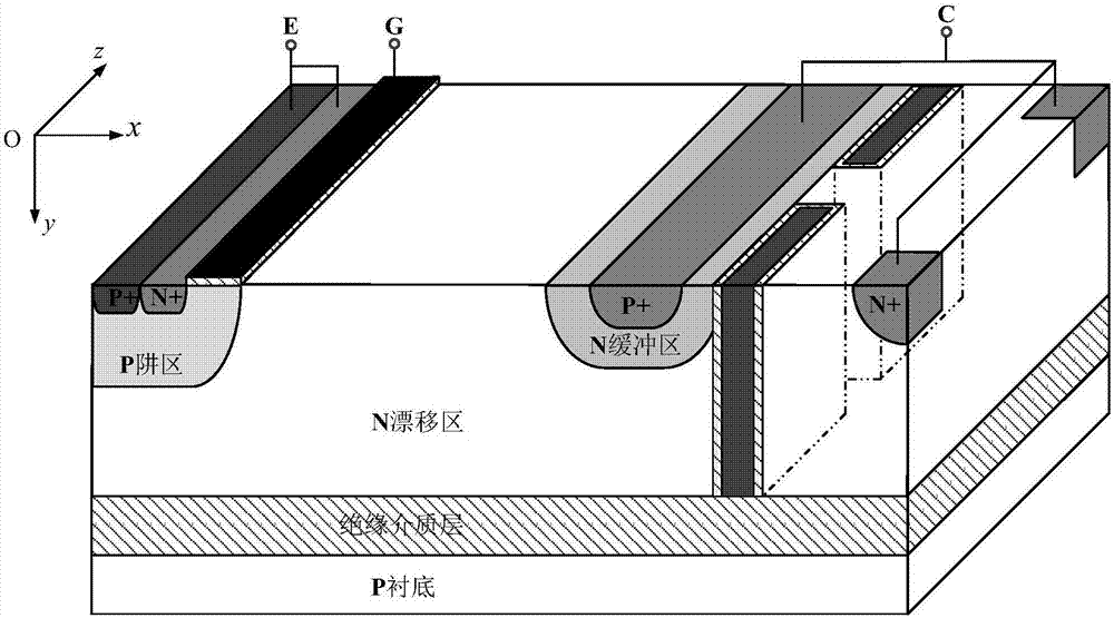
[0030] Such as Figure 5 As shown, the difference between this example and Example 1 is that in this example, an N-type buffer layer 11 is introduced at the end of the collector structure, and the collector groove structure traverses through the N+ collector region 10, the P+ collector region 9 and the N-type The buffer layer 11 extends into the N-type drift region 3 , and its longitudinal depth is greater than that of the N-type buffer layer 11 . When the device is forward-conducting, its working mechanism is consistent with that in Example 1; when the new device is turned off, the bias voltage of the groove collector relative to the collector is a positive potential, and a high-concentration N-type accumulation layer is formed on the side wall of the collector groove , at this time, the collector groove, the N-type accumulation layer on the groove wall and the N-type buffer layer 11 together play an electric field stop function, so that the device can withstand high withstan...

Embodiment 3

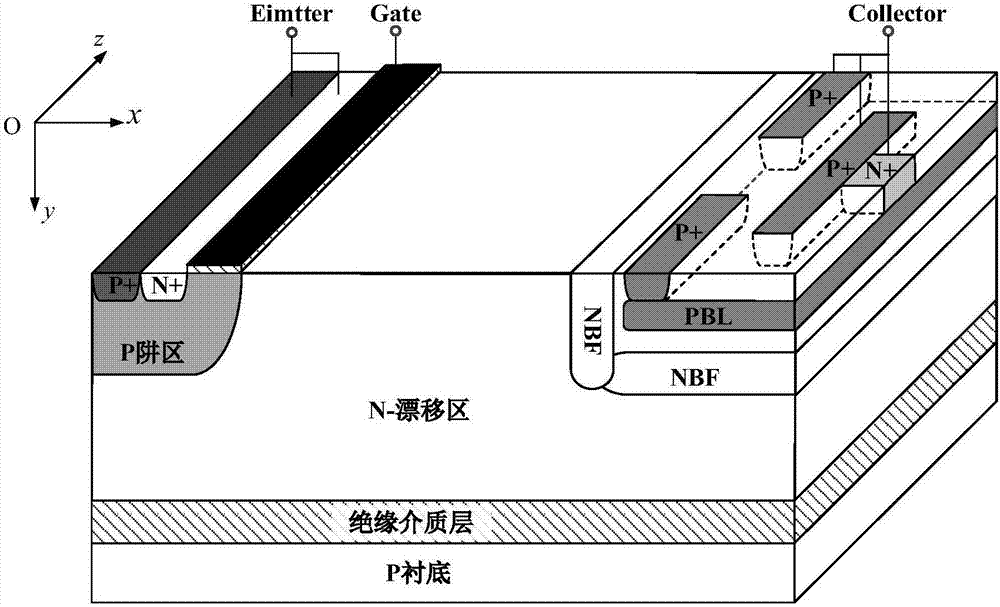
[0032] Such as Figure 6 As shown, the difference between this example and Example 2 is that in this example, the lower surface of the trench dielectric layer 12 in the collector trench structure is connected to the upper surface of the insulating dielectric layer 2 . Compared with Example 2, the new device in this example can obtain higher hole injection efficiency and lower forward conduction voltage drop.


PUM


Abstract

The invention belongs to the technical field of power semiconductors, and specifically relates to an SOI LIGBT with a controllable collector trough. Compared with a conventional structure, the LIGBT mainly introduces a controllable collector trough structure to a collector end and introduces a plurality of trough grid structures to the collector. During the forwarding conduction, the bias voltage of a trough collector relative to the collector is negative, and a side wall of the collector trough forms a high-density P-type reflection layer so as to increase the hole implantation. The segmented trough grid structures serve as the blocking layers of hole extraction. Therefore, the increase of the hole/electron concentration in a drift region facilitates the obtaining of a lower forwarding conduction voltage drop. Meanwhile, because an N+ collector region is located on the upper surface of a P+ collector region and does not make contact with an N-type drift region, a new device does not has a voltage turning-back effect. The beneficial effects of the invention are that the LIGBT, compared with a conventional short-circuit anode-LIGBT structure, is higher in switching-off speed and lower in forwarding conduction voltage drop, and does not have the voltage turning-back effect.

Description

technical field [0001] The invention belongs to the technical field of power semiconductors, and relates to a SOI LIGBT (Lateral Insulated Gate Bipolar Transistor, lateral insulated gate bipolar transistor) with a controllable collector groove. Background technique [0002] Insulated gate bipolar transistor (IGBT) is a new type of power electronic device that is equivalently combined with MOSFET field effect and bipolar junction transistor (BJT). It has both the advantages of high input impedance and simple driving of MOSFET, as well as the advantages of high current density and low conduction voltage drop of BJT devices, and has become one of the core electronic components in modern power electronic circuit applications. Because of its unique advantages in the field of high voltage and high current, IGBT devices are widely used in transportation, smart grid, household appliances, industry, medicine, aerospace and many other fields. [0003] Because LIGBT is well compatible...

Claims


Application Information

Patent Timeline
Patent Type & Authority Applications(China)
IPC IPC(8): H01L29/739H01L29/08
CPCH01L29/0821H01L29/7394
Inventor 罗小蓉魏杰黄琳华邓高强赵哲言刘庆曹厚华孙燕莫日华曾莉尧
Owner UNIV OF ELECTRONICS SCI & TECH OF CHINA
Why Eureka
Try Eureka