Bulk acoustic resonator based on mono-crystal piezoelectric film and preparation method thereof

A technology of bulk acoustic wave resonator and piezoelectric film, which is applied in the direction of electrical components, impedance networks, etc., can solve the problems of low surface uniformity of single crystal LiNbO3 film, impracticality, and poor surface uniformity of thin slices limited by thickness, and achieve Improve the electromechanical coupling coefficient and quality factor, high Q value, and improve the effect of electromechanical coupling coefficient

Active Publication Date: 2017-11-10
ZHEJIANG UNIV
View PDF7 Cites 29 Cited by
  • Summary
  • Abstract
  • Description
  • Claims
  • Application Information

AI Technical Summary

Problems solved by technology

In addition, the surface uniformity of the single crystal LiNbO3 film is low, resulting in a Q value of only 64, which is not practical
The Chinese patent application CN 201610489078A published on December 7, 2016 "thin film bulk acoustic resonator based on single crystal lithium niobate flakes and its preparation method" uses etching to thin lithium niobate, and the thickness of lithium niobate is 5um , this method also has the disadvantages of thickness limitation and poor uniformity of the sheet surface

Method used


Image

  • Bulk acoustic resonator based on mono-crystal piezoelectric film and preparation method thereof
  • Bulk acoustic resonator based on mono-crystal piezoelectric film and preparation method thereof
  • Bulk acoustic resonator based on mono-crystal piezoelectric film and preparation method thereof

Examples


Embodiment 1

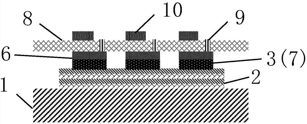
[0052] refer to figure 1 The bulk acoustic wave resonator based on the single crystal piezoelectric thin film of the present invention is described, figure 1 A cross-sectional view of a bulk acoustic wave resonator structure is shown.

[0053] Such as figure 1 As shown, the structure of the bulk acoustic wave resonator based on the single crystal piezoelectric thin film of the present invention is as follows:

[0054] A bulk acoustic wave resonator based on a single crystal piezoelectric thin film includes: a substrate 1, an acoustic reflection layer 2 formed on the substrate 1, and a piezoelectric sandwich structure covering the acoustic reflection layer. The piezoelectric sandwich structure includes sequentially stacked The lower electrode 6, the single crystal piezoelectric film 8, and the upper electrode 10; the single crystal piezoelectric film 8 is provided with a vertical through hole 9 electrically interconnected with the lower electrode 6; the vertical through hole ...

Embodiment 2

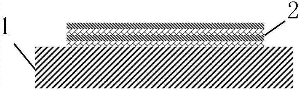
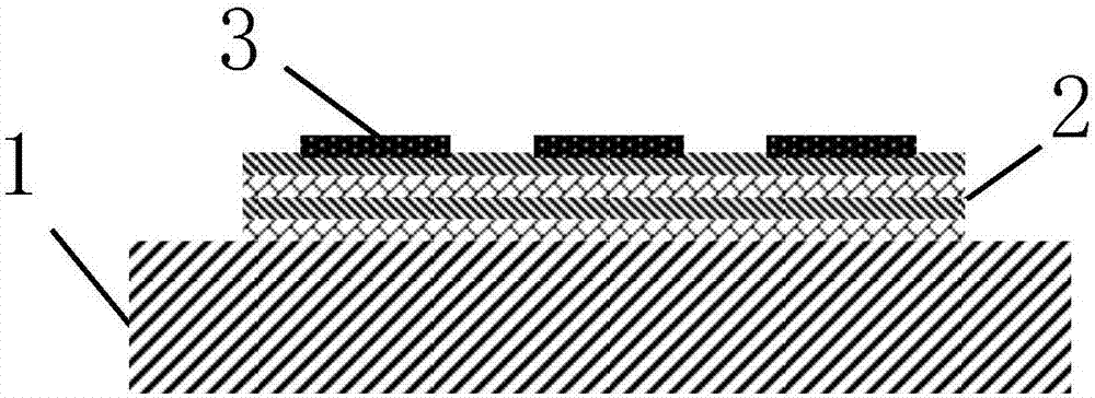
[0064] refer to Figure 2 to Figure 10 The preparation method of the bulk acoustic wave resonator based on the single crystal piezoelectric film of the present invention is described, Figure 2 to Figure 10 It shows the cross-sectional view of the structure obtained by sequential implementation of the method for preparing the bulk acoustic wave resonator.

[0065] The present invention is based on the bulk acoustic wave resonator of single crystal piezoelectric thin film, and its preparation method comprises the following steps:

[0066] S101, using magnetron sputtering and plasma chemical vapor deposition (PECVD) methods to alternately deposit 4 to 7 layers of high acoustic impedance material tungsten and low acoustic impedance material silicon dioxide on the surface of silicon substrate 1, each layer The thickness is 300nm, forming the Bragg acoustic reflection layer 2, such as figure 2 shown;

[0067] S102, on the surface of the Bragg reflection layer 2, deposit a 10nm ...

Embodiment 3

[0076] refer to Figure 11 The structure of the G-S-G coplanar line standard device of the bulk acoustic wave resonator of the present invention is described, and the bulk acoustic wave resonator is prepared by the method described in Example 2, Figure 11 It is a top view of the device G-S-G coplanar line standard device structure.

[0077] Such as Figure 11 As shown, the two common ground electrodes 11 and the vertical through hole 9 electrically interconnected with the lower electrode form a G-S-G coplanar line standard device structure, or the two common ground electrodes 11 and the upper electrode 10 form a G-S-G coplanar line standard device structure.

[0078] The upper electrode 10 adopts an irregular polygon to reduce the influence of parasitic capacitance.


PUM

PropertyMeasurementUnit
Thicknessaaaaaaaaaa
Thicknessaaaaaaaaaa
Thicknessaaaaaaaaaa

Abstract

The invention discloses a bulk acoustic resonator based on a mono-crystal piezoelectric film. The bulk acoustic resonator includes a substrate, an acoustic reflection layer formed on the substrate, and a piezoelectric sandwich structure covering the acoustic reflection layer. The piezoelectric sandwich structure includes a lower electrode, a mono-crystal piezoelectric film, and an upper electrode. A metal film is deposited on the surface of the lower electrode and on the acoustic reflection layer, and a patterned bonding fulcrum is formed through a lithography process, and therefore, the piezoelectric sandwich structure and the acoustic reflection layer are bonded at low temperature. The mono-crystal piezoelectric film is obtained through crystal ion slicing, and the thickness of the film can be controlled by controlling the energy of ion implantation and the ion dose. The bulk acoustic resonator prepared in the invention has an electromechanical coupling coefficient above 44% and a quality factor above 2500, and can play an important role in the modern communication system featuring high-bandwidth and large-capacity data transmission.

Description

technical field [0001] The invention belongs to the technical field of radio frequency micro-electromechanical systems, and in particular relates to a bulk acoustic wave resonator based on a single crystal piezoelectric film and a preparation method thereof. Background technique [0002] With the advancement of micro-electromechanical system technology, thin-film bulk acoustic wave filters have gradually replaced traditional surface acoustic wave filters and ceramic filters due to their small size, low insertion loss, high resonance frequency, high quality factor, and large power capacity. , seized the main market share of communication system filter chips, and met the future high-bandwidth and large-capacity data transmission needs. For example, the US patent US 6515558 (B1) "Thin-film bulk acoustic resonator with enhanced power handling capacity" published on February 4, 2003 provides a thin film bulk acoustic resonance with high power capacity by optimizing the structure ...

Claims


Application Information

Patent Timeline
IPC IPC(8): H03H9/17H03H3/02
CPCH03H3/02H03H9/174H03H2003/023
Inventor 董树荣许红升轩伟鹏骆季奎乌玛·儒可
Owner ZHEJIANG UNIV
Why Eureka
Try Eureka