Method of manufacturing inorganic quantum dot light emitting diode device

A quantum dot light-emitting and diode technology, which is used in the manufacture of semiconductor/solid-state devices, electric solid-state devices, semiconductor devices, etc., can solve the problems of difficult injection of electrons and holes into the light-emitting layer, low exciton recombination efficiency, and high device operating voltage. , to achieve the effect of low preparation difficulty, good charge injection and transfer ability, and stable device performance

Active Publication Date: 2017-12-01
SUZHOU UNIV
View PDF10 Cites 7 Cited by
  • Summary
  • Abstract
  • Description
  • Claims
  • Application Information

AI Technical Summary

Problems solved by technology

[0002] In planar light-emitting semiconductor devices, the energy gap between layers is very large, especially between the electrodes and the organic and inorganic interfaces, which makes it difficult for electrons and holes to inject into the light-emitting layer, and excitons recombine less efficient
Due to the large interface barrier of the device, it is more difficult for electrons to be injected from indium tin oxide (ITO) to the electron transport layer, and from the electron transport layer to the light-emitting layer, which makes the operating voltage of the device very high and the efficiency is very low

Method used


Image

  • Method of manufacturing inorganic quantum dot light emitting diode device
  • Method of manufacturing inorganic quantum dot light emitting diode device
  • Method of manufacturing inorganic quantum dot light emitting diode device

Examples


Embodiment 1

[0028] A preparation of an inorganic quantum dot light-emitting diode device, the preparation steps of the method are as follows:

[0029] Step 1: Rinse the ITO transparent conductive glass substrate in deionized water first, then wash it repeatedly with deionized water, acetone, and ethanol three times, and bake it in a clean environment until the water is completely removed;

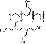
[0030] The second step: PEIE is diluted with ethanol to a concentration of 0.1 wt%, and then coated with PEIE solution on the ITO transparent conductive glass substrate to form a PEIE film layer of about 10 nm;

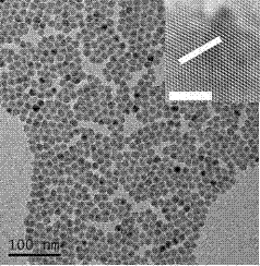
[0031] The third step: PEIE was mixed into the ZnO nanoparticle solution with a doping concentration of 0.1 wt%, and then the mixed solution of ZnO:PEIE was coated on the substrate to form a ZnO:PEIE film layer with a thickness of 60 nm, wherein ZnO The nanoparticle solution is prepared by a common process, which is prepared by the mixed reaction of zinc acetate and tetramethylammonium hydroxi...

Embodiment 2

[0035] The difference between Example 2 and Example 1 is that the concentration of the ethanol solution in the second step is 0.05 wt%, and a PEIE film layer of about 5 nm is formed.

Embodiment 3

[0037] The difference between Example 3 and Example 1 is that the concentration of the mixed solution of ZnO:PEIE in the third step is 0.05 wt%, and the thickness of the film layer is 50 nm.


PUM

PropertyMeasurementUnit
thicknessaaaaaaaaaa
diameteraaaaaaaaaa
thicknessaaaaaaaaaa

Abstract

The invention provides a method of manufacturing a high-efficiency inorganic quantum dot light emitting diode device. The method comprises the following steps: an ITO transparent conductive glass substrate is cleaned and dried; PEIE is diluted by using ethanol to a concentration of 0.05-0.1 wt%, and a PEIE solution is then applied to the substrate to form a thin film around 10 nm; the PEIE is then doped to a ZnO solution, the doping concentration is 0.05-0.1 wt%, and a mixed solution of ZnO:PEIE is applied to the substrate; inorganic quantum dots dissolved in toluene are then applied; and the substrate is finally placed in a vacuum chamber, vacuum evaporation of CBP, CBP:MoO3, MoO3 and Al is carried out sequentially, and a quantum dot light emitting diode device is thus obtained. PEIE/ZnO:PEIE is adopted as an electron injection layer, the injection barrier of electrons is reduced, the electron injection efficiency is improved, and the whole efficiency of the device is greatly improved.

Description

technical field [0001] The invention relates to the field of semiconductor devices, in particular to a method for preparing an inorganic quantum dot light-emitting diode device. Background technique [0002] In planar light-emitting semiconductor devices, the energy gap between layers is very large, especially between the electrodes and the organic and inorganic interfaces, which makes it difficult for electrons and holes to inject into the light-emitting layer, and excitons recombine less efficient. Due to the large interface barrier of the device, it is more difficult for electrons to be injected from indium tin oxide (ITO) to the electron transport layer, and from the electron transport layer to the light-emitting layer, which makes the operating voltage of the device very high and the efficiency is very low. Therefore, in the process of device preparation, it is often necessary to use an interface modification layer between the electron transport layer and the electrode...

Claims


Application Information

Patent Timeline
Patent Type & Authority Applications(China)
IPC IPC(8): H01L51/50H01L51/56
CPCH10K50/115H10K50/171H10K50/16H10K71/00
Inventor 廖良生石英力胡云梁丰
Owner SUZHOU UNIV
Why Eureka
Try Eureka