An organic electroluminescent device
A technology for electroluminescent devices and light-emitting devices, which is applied in the fields of electro-solid devices, electrical components, semiconductor devices, etc., can solve the problems of unclear mechanism of action, difficulty in long-term storage and use, and unfavorable industrial production, and achieves vapor deposition atmosphere. Stable, easy to store and use, beneficial to industrial production
- Summary
- Abstract
- Description
- Claims
- Application Information
AI Technical Summary
Problems solved by technology
Method used
Image
Examples
Embodiment 1
[0062] The structure of a single-electron device:
[0063] ITO / BCP(10nm) / Bphen(90nm) / 10%M-ETM(10nm) / Al;
[0064] First electrode layer 02 (anode ITO) / hole transport layer 05 (BCP) / hole blocking layer 07 (Bphen) / electron transport layer 08 (10% M-ETM) / second electrode layer 03 (cathode Al)
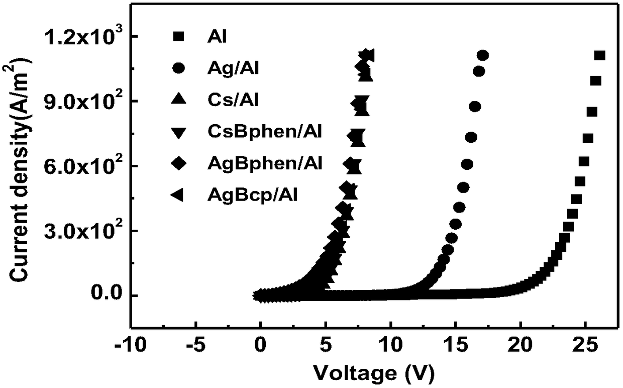
[0065] The host material of the electron transport layer in this embodiment is Bphen, the inert metal doped is Ag, and the active metal Cs (obtained by decomposing cesium carbonate in vacuum) is used in the comparative device. Such as figure 2 As shown, device 1 is the curve corresponding to Al, device 2 is the curve corresponding to Ag / Al, device 3 is the curve corresponding to Cs / Al, device 4 is the curve corresponding to CsBphen / Al, and device 5 is the curve corresponding to AgBphen / Al , device 6 is the curve corresponding to AgBcp / Al, and the cathodes of devices 1-6 are all Al, where:
[0066] The electron transport layer 08 of the device 1 is Bphen (that is, not doped with an inert...
Embodiment 2
[0077] Device structure:
[0078] ITO / HAT-CN(10nm) / NPB(30nm) / Alq 3 (30nm) / Bphen(20nm) / x%Ag:Bphen 10nm / Ag
[0079] The first electrode layer 02 (anode ITO), the hole injection layer 04 (HAT-CN), the hole transport layer 05 (NPB), the light emitting layer 06 (Alq 3 ), hole blocking layer 07 (Bphen), electron transport layer 08 (x%Ag:Bphen), second electrode layer 03 (cathode Ag);
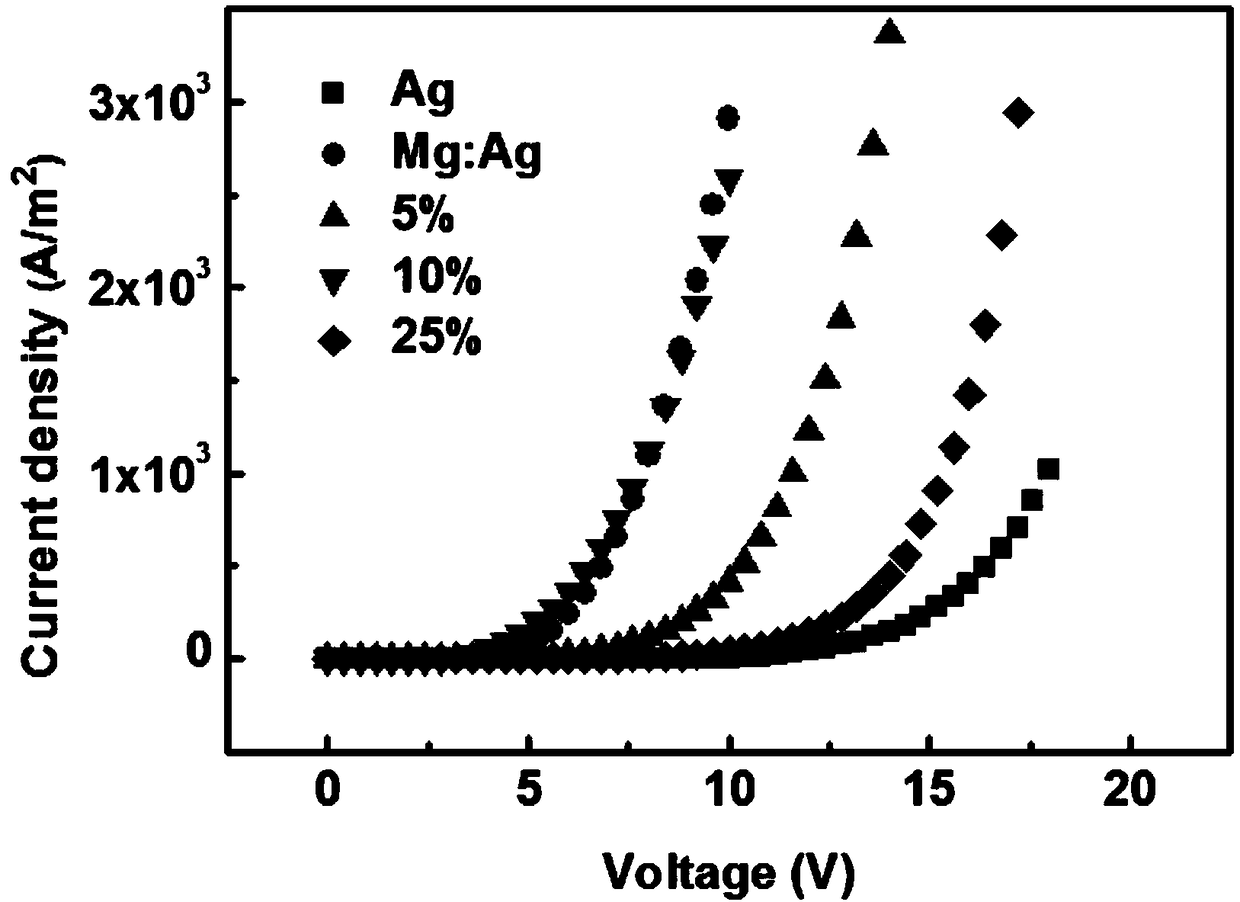
[0080] The host material of the electron transport layer in this embodiment is Bphen, and the doped inert metal is Ag. Such as Figure 3-Figure 6 As shown, device 7 is the curve corresponding to Ag, device 8 is the curve corresponding to Mg:Ag, device 9 is the curve corresponding to 5%, device 10 is the curve corresponding to 10%, device 11 is the curve corresponding to 25%, device 7 And Ag in device 8, Mg:Ag is metal cathode respectively, and its electron transport layer material is Bphen; The metal cathode of device 9, device 10 and device 11 is Ag;
[0081] in:
[0082] The electron transport...
Embodiment 3
[0087] Device structure:
[0088] ITO / HATCN(10nm) / NPB(30nm) / Alq 3(30nm) / Bphen(20nm) / x%Ag-Bphen 10nm / Mg:Ag / Ag
[0089] The first electrode layer 02 (anode ITO), the hole injection layer 04 (HATCN), the hole transport layer 05 (NPB), the light emitting layer 06 (Alq 3 ), hole blocking layer 07 (Bphen), electron transport layer 08 (x%Ag-Bphen), second electrode layer 03 (cathode Mg:Ag / Ag);
[0090] The host material of the electron transport layer in this embodiment is Bphen, and the doped inert metal is Ag. Such as Figure 7-Figure 10 As shown, device 12 is the curve corresponding to Ag, device 13 is the curve corresponding to Mg:Ag, device 14 is the curve corresponding to 5%, device 15 is the curve corresponding to 10%, device 16 is the curve corresponding to 20%, device 12 And Ag in device 13, Mg:Ag is metal cathode respectively, and its electron transport layer material is Bphen; The metal cathode of device 14, device 15 and device 16 is Ag;
[0091] Wherein: the materia...
PUM
 Abstract
Description
Claims
Application Information
 - R&D
- Intellectual Property
- Life Sciences
- Materials
- Tech Scout
- Unparalleled Data Quality
- Higher Quality Content
- 60% Fewer Hallucinations
Browse by: Latest US Patents, China's latest patents, Technical Efficacy Thesaurus, Application Domain, Technology Topic, Popular Technical Reports.
© 2025 PatSnap. All rights reserved.Legal|Privacy policy|Modern Slavery Act Transparency Statement|Sitemap|About US| Contact US: help@patsnap.com


