A kind of preparation method of thin film bulk acoustic resonator

A thin-film bulk acoustic wave and resonator technology, applied in impedance networks, electrical components, etc., can solve the problems of lower electrode damage, high surface flatness requirements, and difficulty in meeting hydrophilic bonding, and achieve the structural strength of the prepared device. The effect of large and simple preparation process

Active Publication Date: 2021-06-01
CHIMEMS MICROELECTRONICS CO LTD
View PDF6 Cites 0 Cited by
  • Summary
  • Abstract
  • Description
  • Claims
  • Application Information

AI Technical Summary

Problems solved by technology

[0006] However, due to the hydrophilic bonding to SiO 2 The surface flatness of the bonding layer is very high, so it is difficult to pattern the bottom electrode in the bulk acoustic wave resonator stack structure, otherwise the SiO grown on the patterned bottom electrode 2 The bonding layer will show large surface fluctuations, which is difficult to meet the needs of hydrophilic bonding
And due to SiO 2 The thickness of the bonding layer is usually less than 2μm, if the SiO 2 Layer chemical mechanical polishing (CMP), it is easy to cause damage to the lower electrode
Since the lower electrode pattern of the thin film bulk acoustic resonator needs to be specially designed to achieve the effect of suppressing clutter, but the preparation of LiNbO by hydrophilic bond transfer 3 Piezoelectric layer technology is difficult to prepare patterned thin film bulk acoustic resonator stack structure

Method used


Image

  • A kind of preparation method of thin film bulk acoustic resonator
  • A kind of preparation method of thin film bulk acoustic resonator
  • A kind of preparation method of thin film bulk acoustic resonator

Examples


Embodiment Construction

[0028] The present invention will be described in further detail below in conjunction with the accompanying drawings and embodiments.

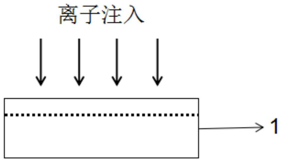
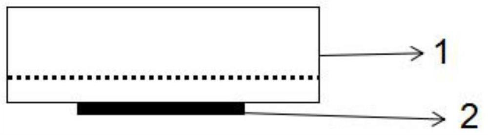
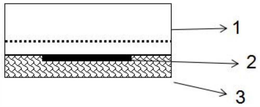
[0029] Step 1. Using an ion implanter to single crystal LiNbO 3 The wafer is implanted with He ions, the implantation energy is 150keV~285kV, and the implantation dose is greater than 2×10 16 ions / cm 2 , injecting He+ in LiNbO 3 A He+ accumulation layer is formed under the wafer surface. The depth of the accumulation layer depends on the implantation energy. The implantation depth is 600-900nm, such as figure 1 As shown, the dotted line indicates the location of the aggregation layer.

[0030] Step 2, in LiNbO 3 Inject a thin layer of Ti with a thickness of 10nm as the adhesion layer, and then grow a thin layer of Al with a thickness of 50-200nm on the thin layer of Ti as the lower electrode. The growth methods of the Ti thin layer and the Al thin layer include electron beam evaporation, Resistance evaporation, DC sputtering, magnetron sput...


PUM

PropertyMeasurementUnit
thicknessaaaaaaaaaa
thicknessaaaaaaaaaa
thicknessaaaaaaaaaa

Abstract

The invention relates to the technical field of thin film bulk acoustic resonators, in particular to a preparation method of thin film bulk acoustic wave resonators. The present invention uses polymers for wafer bonding, replacing SiO commonly used in traditional ion implantation stripping methods. 2 Hydrophilic bonding, the electrode covered by the polymer can be patterned according to the design requirements of the thin film bulk acoustic resonator, due to the fluidity of the polymer, it can be self-planarized under the action of pressure during the wafer bonding process, and the pattern Electrodes can be nested in polymers and are not suitable for LiNbO 3 The peeling of the single crystal thin film does not cause any impact, which solves the problem that the lower electrode is difficult to pattern during the bonding transfer process of the single crystal thin film. At the same time, the polymer is used as the acoustic reflection layer of the film bulk acoustic resonator, which solves the problems of low structural strength of the air resonator and the difficulty of preparing the Bragg acoustic reflection cavity, and the preparation process of the device is simple, and the prepared device has a strong structure.

Description

technical field [0001] The invention relates to the technical field of thin-film bulk acoustic wave resonators, in particular to a method for preparing a single-crystal piezoelectric thin-film type bulk acoustic wave resonator with a solid-state acoustic reflection layer. Background technique [0002] A film bulk acoustic resonator (FBAR) is a piezoelectric thin film resonator. The basic structure of the film bulk acoustic resonator is a laminated structure consisting of an upper electrode, a piezoelectric layer and a lower electrode on the substrate; in order to suppress the dissipation of vibration energy, a cavity or a Bragg reflection layer is provided below the laminated structure. There are two methods for preparing the cavity: one is to etch the substrate area under the stacked structure, and the etching is carried out from the back of the substrate; the other is to make a patterned surface sacrificial layer on the surface of the substrate, and after preparing the sta...

Claims


Application Information

Patent Timeline
Patent Type & Authority Patents(China)
IPC IPC(8): H03H3/02H03H9/17
CPCH03H3/02H03H9/171H03H2003/023
Inventor 帅垚龚朝官白晓圆罗文博吴传贵张万里
Owner CHIMEMS MICROELECTRONICS CO LTD
Why Eureka
Try Eureka