Gallium nitride surface emitting laser based on silicon nitride photonic crystal and preparation method

A technology for emitting lasers and photonic crystals, which is applied in the field of gallium nitride surface emitting lasers and its preparation, which can solve the problems of device design, processing and preparation, and performance limitations, and achieve the effects of excellent performance and high optical field coupling efficiency.

Pending Publication Date: 2022-02-25
NANJING UNIV OF POSTS & TELECOMM
View PDF15 Cites 0 Cited by
  • Summary
  • Abstract
  • Description
  • Claims
  • Application Information

AI Technical Summary

Problems solved by technology

In the existing gallium nitride photonic crystal lasers, the photonic crystal structure is introduced into the gallium nitride material. There are buried photonic crystal lasers and surface-etched photonic crystal lasers. The design, processing and performance of the devices are restricted

Method used


Image

  • Gallium nitride surface emitting laser based on silicon nitride photonic crystal and preparation method
  • Gallium nitride surface emitting laser based on silicon nitride photonic crystal and preparation method

Examples


Embodiment 2

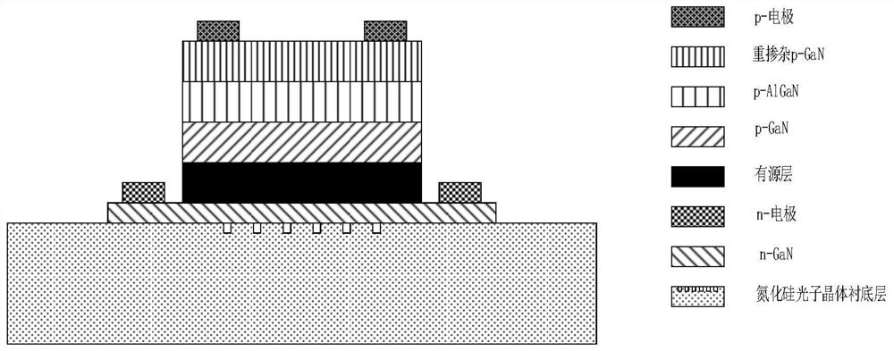
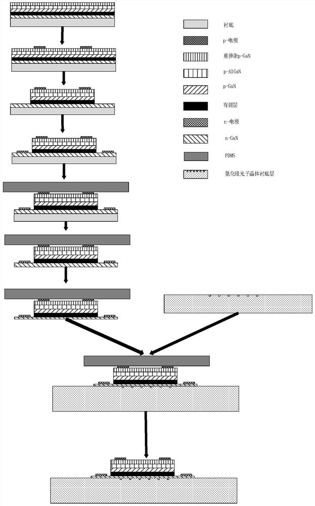
[0060] same as figure 1 As shown, the fabrication method of gallium nitride surface-emitting laser based on silicon nitride photonic crystal includes:

[0061] Silicon nitride photonic crystal substrate layer;

[0062] The n-GaN layer is located on the silicon nitride photonic crystal substrate layer;

[0063] The active layer is located on the n-GaN layer, and the active layer is a multi-layer quantum well layer composed of InGaN / GaN pairs;

[0064] a p-GaN layer overlying the active layer;

[0065] a p-AlGaN layer located on the p-GaN layer;

[0066] A heavily doped p-GaN layer on top of the p-AlGaN layer;

[0067] n-electrode, on the surface of the n-GaN layer;

[0068] The p-electrode, on the surface of the heavily doped p-GaN layer.

[0069] The silicon nitride photonic crystal layer is a structure in which the silicon nitride layer is carved through to form periodic holes. The lattice type of the photonic crystal is square lattice or triangular lattice or honeycomb l...


PUM

PropertyMeasurementUnit
radiusaaaaaaaaaa
thicknessaaaaaaaaaa
thicknessaaaaaaaaaa

Abstract

The invention provides a gallium nitride surface emitting laser based on a silicon nitride photonic crystal and a preparation method. The gallium nitride surface emitting laser structurally comprises a silicon nitride photonic crystal substrate layer, an n-GaN layer, an n-electrode, a quantum well active layer formed by InGaN / GaN in pairs, a p-GaN layer, a p-AlGaN layer, a p-GaN heavily doped layer and a p-electrode. A structure in which the photonic crystal layer of silicon nitride with low-loss resonance is combined with the active film cavity of GaN is formed by using a film transfer process, so that the blue-light band laser with innovative performance is realized. The photonic crystal based on the silicon nitride material is simpler and more convenient to grow and prepare, high Q value and low loss are achieved, meanwhile, efficient coupling between the photonic crystal layer and an active layer light field can be achieved through combination of the photonic crystal and the gallium nitride thin film, and implementation of a high-performance laser is facilitated.

Description

technical field [0001] The invention discloses a gallium nitride surface-emitting laser based on a silicon nitride photonic crystal and a preparation method thereof, and belongs to the field of active photonic devices. Background technique [0002] Photonic crystal surface-emitting laser (PCSEL) is a new type of semiconductor laser that can achieve extremely low divergence angle (less than 1°) and high-power laser output. It is used in lidar, space communication, high-density storage, sensing and laser processing. It has important application prospects. Gallium nitride (GaN), as a representative of wide bandgap semiconductor materials, has high application value. Due to the excellent photoelectric properties of gallium nitride, and with the development of material growth technology, gallium nitride-based photonic crystal lasers have more application requirements in more and more fields, such as the application of blue and green lasers. In the existing gallium nitride photo...

Claims


Application Information

Patent Timeline
Patent Type & Authority Applications(China)
IPC IPC(8): H01S5/11H01S5/343
CPCH01S5/11H01S5/34333
Inventor 刘启发周扬
Owner NANJING UNIV OF POSTS & TELECOMM
Why Eureka
Try Eureka