

Method for tuning forbidden band width of Ga2O3 through Nb doping
A bandgap, ga2o3 technology, applied in the field of semiconductor materials, to achieve the effect of large bandgap tuning range
- Summary
- Abstract
- Description
- Claims
- Application Information
AI Technical Summary
Problems solved by technology
Method used
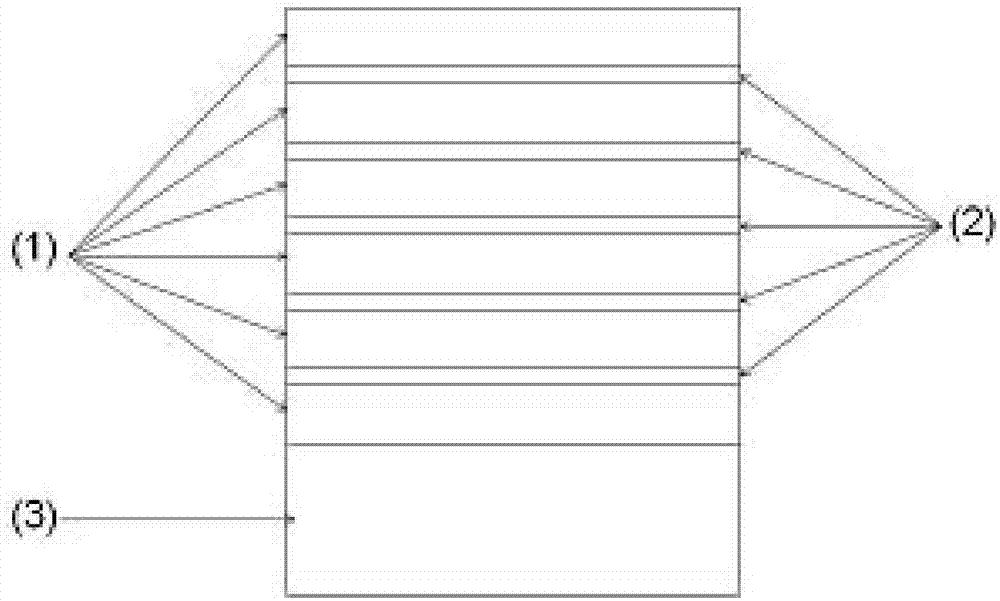
Image

Examples
Embodiment 1
[0021] (1) A polished n-type silicon wafer is used as a substrate (with a resistivity of 2-4Ωcm and a thickness of 0.3mm). The substrates were ultrasonically cleaned with toluene, acetone, ethanol and deionized water for 15 min, and then dried in a glove box for 1 hour.
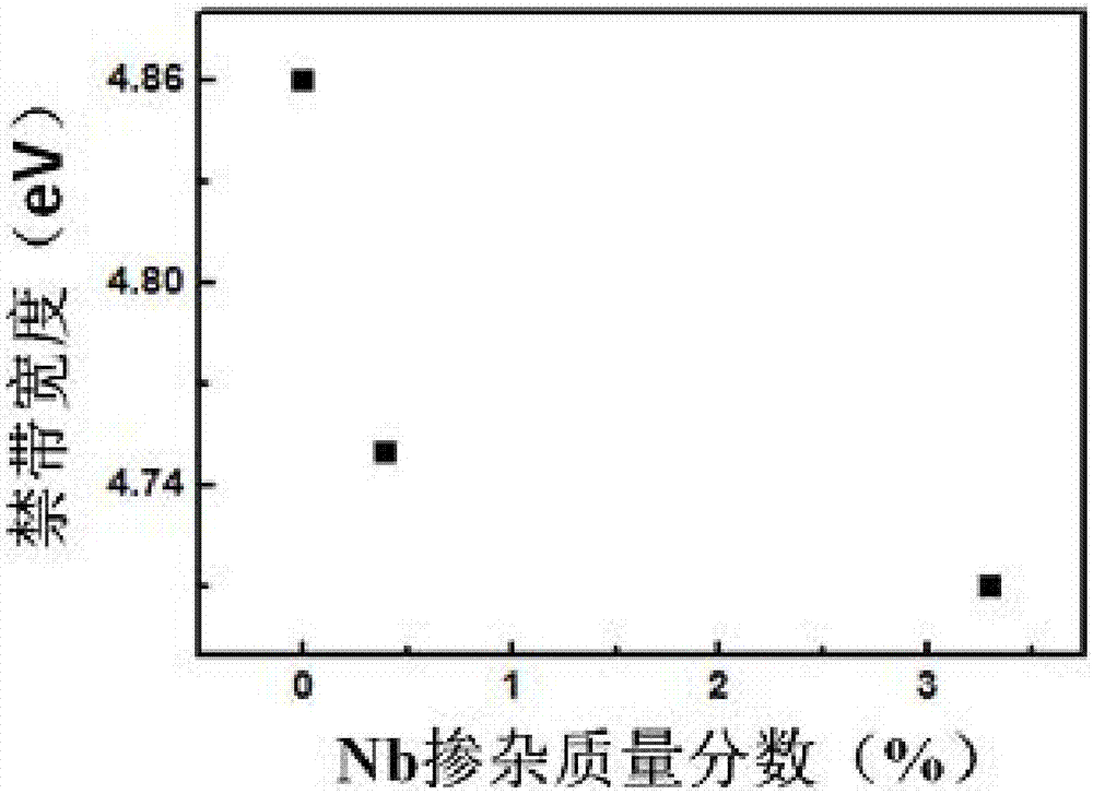
[0022] (2) Using radio frequency magnetron sputtering equipment to deposit Nb: Ga in layered growth 2 o 3 thin film materials, by controlling the Nb 2 o 5 and Ga 2 o 3 The sputtering time of the target controls the Nb doping dose. The pre-vacuum degree of the system is 1×10 -3 Below Pa. The film growth atmosphere is Ar, and the working pressure is 0.5Pa. Ga 2 o 3 and Nb 2 o 5 The sputtering power of the target is 80W, and the sputtering time is 300s, 10s alternately and 300s, 40s alternately, so as to obtain Nb:Ga with different Nb doping content 2 o 3 Thin film, wherein the thickness of the film is 250-260nm.
[0023] (3) The prepared Nb:Ga 2 o 3 The film samples were placed in a tube furnac...
Embodiment 2
[0026] (1) A polished n-type silicon wafer is used as a substrate (with a resistivity of 2-4Ωcm and a thickness of 0.3mm). The substrates were ultrasonically cleaned with toluene, acetone, ethanol and deionized water for 15 min, and then dried in a glove box for 1 hour.
[0027] (2) Deposit Nb:Ga by co-sputtering using radio frequency magnetron sputtering equipment 2 o 3 film material. The pre-vacuum degree of the system is 1×10 -3 Below Pa. The film growth atmosphere is Ar, and the working pressure is 0.6Pa. Ga 2 o 3 and Nb 2 o 5 The sputtering power of the target is 80W, the sputtering time is 50min, and four Nb:Ga 2 o 3 Film samples.
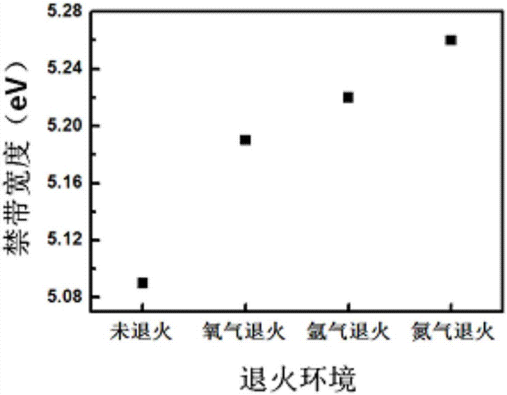
[0028] (3) The prepared 3 Nb:Ga2 o 3 Thin film samples were placed in a tube furnace for Ar, O 2 and N 2 Atmosphere annealing. Use a mechanical pump to evacuate the air pressure in the tube furnace to below 1Pa, and introduce high-purity Ar (99.999%), O 2 (99.999%) or N 2 (99.999%). After that, the working pressure was mainta...
Embodiment 3
[0031] (1) A polished n-type silicon wafer is used as a substrate (with a resistivity of 2-4Ωcm and a thickness of 0.3mm). The substrates were ultrasonically cleaned with toluene, acetone, ethanol and deionized water for 15 min, and then dried in a glove box for 1 hour.
[0032] (2) Deposit Nb:Ga by co-sputtering using radio frequency magnetron sputtering equipment 2 o 3 film material. The pre-vacuum degree of the system is 1×10 -3 Below Pa. The film growth atmosphere is Ar, and the working pressure is 0.6Pa. Ga 2 o 3 and Nb 2 o 5 The sputtering power of the target is 80W. By controlling the co-sputtering coating time, multiple Nb:Ga with the same Nb doping content (doping mass percentage content is 1.5%) but different film thicknesses are obtained. 2 o 3 Film samples. Set the coating time to 20min, 30min, 40min, 60min respectively, and obtain four Nb:Ga films with thicknesses of 100nm, 150nm, 200nm and 300nm respectively. 2 o 3 Film samples.
[0033] (3) The pre...
PUM
| Property | Measurement | Unit |
|---|---|---|
| Resistivity | aaaaa | aaaaa |
| Thickness | aaaaa | aaaaa |
| Thickness | aaaaa | aaaaa |
Abstract
Description
Claims
Application Information