Eureka AIR delivers breakthrough ideas for toughest innovation challenges, trusted by R&D personnel around the world.

Plasma immersion ion implantation doping device and application thereof

A technology of immersion ion implantation and plasma, applied in the field of doping of semiconductor materials or devices, can solve the problems of high cost, adverse material consequences, complex structure, etc., and achieve the effects of low cost, improved purity, and reduced contamination

Active Publication Date: 2017-12-29
PEKING UNIV
View PDF8 Cites 0 Cited by
  • Summary
  • Abstract
  • Description
  • Claims
  • Application Information

AI Technical Summary

Problems solved by technology

However, the structure of the existing plasma immersion ion implantation device is relatively complicated, and the cost is relatively expensive. More importantly, in the doping process, in addition to the impurities required to be doped, there are also a large number of unnecessary impurities from various components of the equipment , is also mixed into the material to be mixed at the same time
These impurities are likely to cause adverse consequences to the material, especially for semiconductors, it is almost intolerable

Method used


Image

  • Plasma immersion ion implantation doping device and application thereof

Examples


Embodiment Construction

[0039] The present invention will be further described in detail through the embodiments below in conjunction with the accompanying drawings.

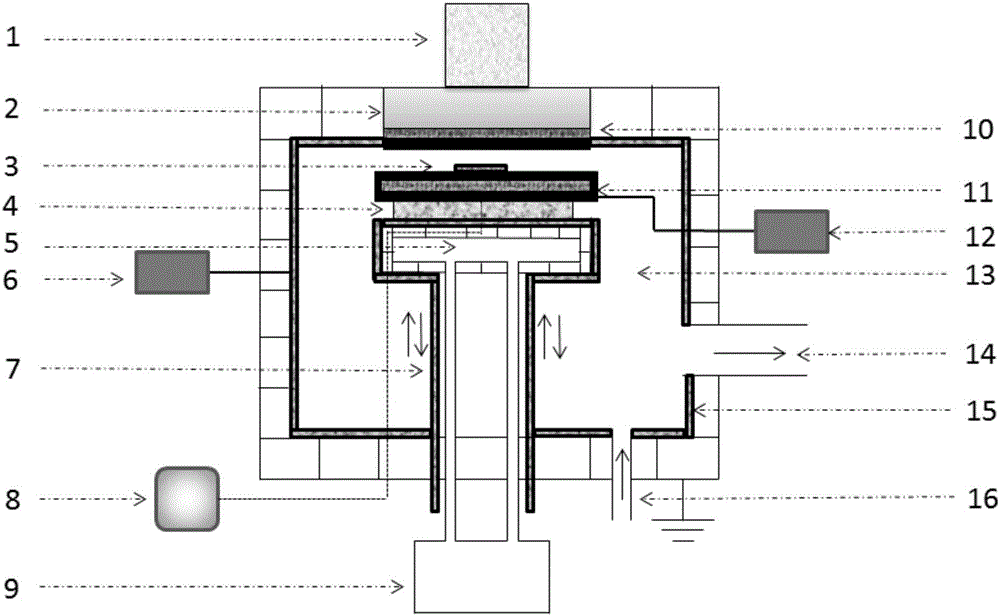
[0040] Such as figure 1 As shown, the parallel plate chamber plasma immersion ion implantation doping device includes: a vacuum chamber 13 , a plasma coupling window 2 located on the top of the vacuum chamber 13 , and a plasma generating unit 1 located above the plasma coupling window 2 . The upper plate 10 of the parallel plate chamber, that is, the upper substrate coated with a doped impurity deposition layer, is close to the plasma coupling window 2 above; the lower plate 11 of the parallel plate chamber, that is, the lower substrate coated with a doped impurity deposition layer, the lower Clinging to the insulator 4 on the hollow metal box 5. The hollow metal box 5 is located on the liftable support 7, and the cavity is filled with a temperature-controlled liquid, and its temperature is controlled at 0°C-300°C by a liquid circulat...


PUM

PropertyMeasurementUnit
thicknessaaaaaaaaaa
thicknessaaaaaaaaaa
thicknessaaaaaaaaaa

Abstract

The invention discloses a plasma immersion ion implantation doping device and application of the plasma immersion ion implantation doping device. According to the plasma immersion ion implantation doping device, a plasma generating unit and a plasma coupling window are arranged on the top of a vacuum cavity. A parallel plate cavity is formed below the plasma coupling window and is next to the plasma coupling window, doping impurity layers are arranged on the surfaces, exposed to the vacuum cavity, of an upper plate and a lower plate of the parallel plate cavity in a deposition mode, and the lower plate is connected with a direct-current voltage source which provides negative bias voltage. A double-layer lining material covers the exposed inner surface of the vacuum cavity, the outer layer is a contamination-preventing layer, the inner layer is an insulating layer, and the contamination-preventing layer is connected with a direct-current voltage source which provides positive bias voltage. A semiconductor material or device to be doped is arranged in the parallel plate cavity. The plasma immersion ion implantation doping device is simple in structure and low in cost, the contamination caused by non-doping impurities on the semiconductor material or device to be doped is reduced to the maximum extent, and the degree of purity of ion implantation doping is greatly improved.

Description

technical field [0001] The invention relates to the doping technology of semiconductor materials or devices, in particular to a device for doping semiconductors by plasma immersion ion implantation in a parallel plate cavity and its application. Background technique [0002] The doping process is to add the required impurities into a specific area near the surface of solid materials such as semiconductors and metals or devices to achieve a certain surface concentration and depth, thereby changing the physical and chemical properties of materials or devices. For semiconductors, the doping process can be used to make PN junctions, source and drain regions of field effect transistors, and can also greatly improve the ohmic contact between metals and semiconductors. There are three main types of impurities doped into semiconductors: the first type is shallow acceptor impurities or donor impurities that can determine the conductivity type and provide carriers (such as B, P, As in...

Claims


Application Information

Patent Timeline
Patent Type & Authority Applications(China)
IPC IPC(8): C23C14/48
CPCC23C14/48
Inventor 秦国刚宿世臣侯瑞祥徐万劲臧之昊李磊
Owner PEKING UNIV
Why Eureka
Eureka Blog
Learn More