Supercharge Your Innovation With Domain-Expert AI Agents!

Vertical superjunction double-diffused metal oxide semiconductor field effect transistor with composite dielectric layer and manufacturing method thereof

A technology of oxide semiconductor and composite medium, which is applied in semiconductor/solid-state device manufacturing, semiconductor devices, electrical components, etc., and can solve the problems of doping concentration limitation and affecting device conduction loss, etc.

Active Publication Date: 2020-06-16
XIDIAN UNIV
View PDF4 Cites 0 Cited by
  • Summary
  • Abstract
  • Description
  • Claims
  • Application Information

AI Technical Summary

Problems solved by technology

[0004] It can be seen that under a certain N-column width, the maximum doping concentration of the N-column is determined, that is, the doping concentration of the superjunction drift region is limited, thus affecting the conduction loss of the device

Method used


Image

  • Vertical superjunction double-diffused metal oxide semiconductor field effect transistor with composite dielectric layer and manufacturing method thereof
  • Vertical superjunction double-diffused metal oxide semiconductor field effect transistor with composite dielectric layer and manufacturing method thereof

Examples


Embodiment Construction

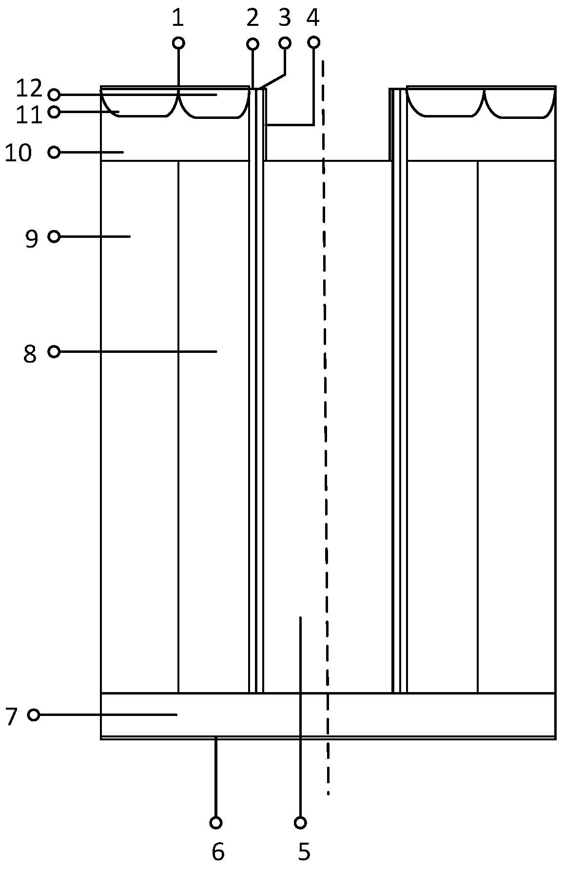
[0045] like figure 1 As shown, the longitudinal super-junction double-diffused metal oxide semiconductor field effect transistor with composite dielectric layer of the present invention:

[0046] The substrate of the element semiconductor material is the drain region 7 of the device, and the doping concentration is 1×10 13 cm -3 ~1×10 15 cm -3 ;

[0047] A superjunction drift region (N-type drift region 8 in epitaxial layer and P-type drift region 9 in epitaxial layer) is formed by subregional epitaxy on the substrate; the width of P pillar in the superjunction drift region is W P with N pillar width W N The typical value of the ratio is 1 / 1 to 5 / 1; the doping concentration of the N column is N D Doping concentration N with P pillar A The typical value of the ratio ranges from 2 / 1 to 10 / 1.

[0048] The base region 10 is formed by further epitaxy and doping on the drift region;

[0049] The trench is etched on the base region, and the bottom of the trench passes throug...


PUM

PropertyMeasurementUnit
widthaaaaaaaaaa
thicknessaaaaaaaaaa
relative permittivityaaaaaaaaaa

Abstract

The invention provides a longitudinal super junction double diffusion metal oxide semiconductor field effect transistor with composite dielectric layer (CDL) and manufacturing method thereof. The device forms the CDL composed of a semi-insulating polysilicon layer (SIPOS) and a high dielectric constant (High K) dielectric layer on the side wall of a drift region under a device gate electrode. Whenthe device is turned off, the SIPOS column and the High K dielectric layer have a uniform electric field, and the electric field is modulated to make the electric field in the super junction drift region of the device be evenly distributed. Meanwhile, the CDL and the super junction assist the consumption of the super junction drift region together, the consumption capability of the super junctiondrift region is greatly improved, so that the doping concentration of the drift region of the device is increased, and the conductive resistance of the device is reduced. When the device is turned on, the drift region has a majority carrier accumulation layer on the sidewall, so that the conductive resistance of the device is further reduced.

Description

technical field [0001] The present invention relates to the field of semiconductor devices, in particular to a trench type vertical double-diffused metal oxide semiconductor field effect transistor. Background technique [0002] With the rapid development of power MOSFET devices representing new power semiconductor devices, power semiconductor devices are widely used in computers, lighting, consumer electronics, automotive electronics, industrial drives and other fields. Power semiconductor devices are the core devices of green, low power consumption, energy saving and environmental protection. For high-voltage MOSFETs, the high energy efficiency requirements of the power supply are the main factors affecting the future development of the product. However, in the high-voltage application field of power devices, as the breakdown voltage of the device increases, the thickness of the power VDMOS epitaxial layer continues to increase, and the doping concentration of the drift r...

Claims


Application Information

Patent Timeline
Patent Type & Authority Patents(China)
IPC IPC(8): H01L29/78H01L29/06H01L21/336
Inventor 段宝兴曹震师通通吕建梅杨银堂
Owner XIDIAN UNIV
Features
  • R&D
  • Intellectual Property
  • Life Sciences
  • Materials
  • Tech Scout
  • Unparalleled Data Quality
  • Higher Quality Content
  • 60% Fewer Hallucinations
Learn More