
A method of manufacturing a planar thermoelectric element

A technology of thermoelectric elements and manufacturing methods, applied in the manufacture/processing of thermoelectric devices, thermoelectric devices that only use the Peltier or Seebeck effect, etc., can solve problems such as the limitation of refrigeration effects, and achieve compact circuit structure, high energy density, and optimized Effect of thermoelectric conversion efficiency

Active Publication Date: 2020-09-15
上海萃励电子科技有限公司
View PDF3 Cites 0 Cited by
  • Summary
  • Abstract
  • Description
  • Claims
  • Application Information

AI Technical Summary

Problems solved by technology

[0003] When using thermoelectric materials for cooling in the temperature control process of different temperature points or temperature sections, it is necessary to adjust the cooling power, but the large current will generate a lot of Joule heat in the circuit during rapid cooling, which greatly limits the cooling effect

Method used


Image

  • A method of manufacturing a planar thermoelectric element
  • A method of manufacturing a planar thermoelectric element
  • A method of manufacturing a planar thermoelectric element

Examples


Embodiment 1

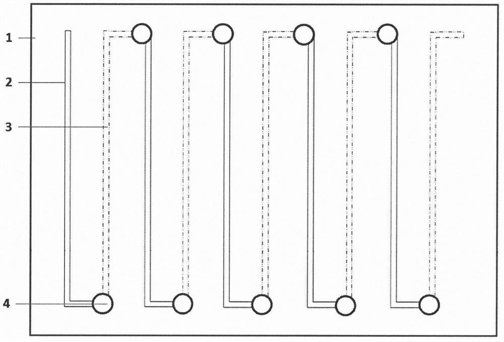
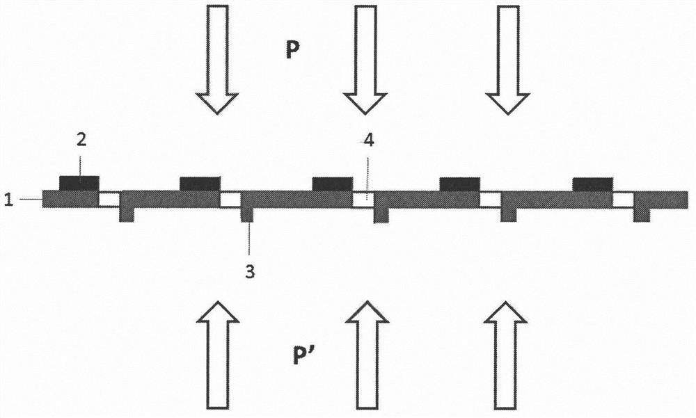
[0018] Lead zirconate titanate piezoelectric ceramics are used as the substrate, and N-type Bi is magnetron sputtered through the mask on the front. 0.5 Sb 1.5 Te 3 Circuit layer of thermoelectric material, P-type Bi sputtered by mask magnetron sputtering on the back 2 Te 2.7 Se 0.3 For the circuit layer of thermoelectric materials, through holes are drilled at the end of the circuit, and copper is electroplated in the through holes to form an alternating series circuit structure of N-P-N-P.... The planar structure is as follows figure 1 shown. When the series circuit is fed with current, one side of the substrate can be cooled and the other side can dissipate heat, forming a temperature difference; when there is a temperature difference between the two ends of the substrate, a potential difference is generated in the alternating series circuit structure, which can convert the temperature difference into electrical energy and output it outward. In the process of thermoele...

Embodiment 2

[0020] Using lead magnesium niobate piezoelectric ceramics as the substrate, the circuit layer of N-type PbTe thermoelectric material vacuum-evaporated through a mask on the front, and the circuit layer of P-type PbSe thermoelectric material vacuum-evaporated through a mask on the back, at the end of the line Drill through holes, electroplate copper in the through holes to form an alternating series circuit structure of N-P-N-P..., the planar structure is as follows figure 1 shown. When the series circuit is fed with current, one side of the substrate can be cooled and the other side can dissipate heat, forming a temperature difference; when there is a temperature difference between the two ends of the substrate, a potential difference is generated in the alternating series circuit structure, which can convert the temperature difference into electrical energy and output it outward. In the process of thermoelectric or electrothermal conversion, normal pressure is applied to the...

Embodiment 3

[0022] P(VDF-TrFE) piezoelectric polymer is used as the substrate, and the N-type poly-3,4 ethylenedioxythiophene: polydiallyldimethylammonium chloride thermoelectric material circuit layer is screen-printed on the front On the back, the circuit layer of polyphenylpyrrole thermoelectric material is filled with P-type graphene printed on the screen, through-holes are drilled at the end of the circuit, and copper is electroplated in the through-holes to form an alternating series circuit structure of N-P-N-P.... The planar structure is as follows figure 1 shown. When the series circuit is fed with current, one side of the substrate can be cooled and the other side can dissipate heat, forming a temperature difference; when there is a temperature difference between the two ends of the substrate, a potential difference is generated in the alternating series circuit structure, which can convert the temperature difference into electrical energy and output it outward. In the process o...


PUM


Abstract

The invention discloses a method for manufacturing a planar thermoelectric element, which is characterized in that: a piezoelectric material is used as a substrate, thermoelectric semiconductor material circuits are printed on the substrate, and circuit layers of N-type and P-type thermoelectric materials are printed on both sides of the substrate. A row of through holes is drilled at both ends of the substrate, and the through holes are plated with metal. The circuit layers on both sides are connected through the through holes plated with metal at both ends to form an alternating series circuit structure of N-P-N-P... to obtain a planar thermoelectric element. The advantage of the present invention is that the planar thermoelectric element circuit produced by this method has a compact structure and high energy density. It uses the piezoelectric material substrate to generate polarization in the normal direction, and can adjust the thermoelectric efficiency and cooling efficiency of the thermoelectric material circuit, especially when improving refrigeration efficiency. The introduction of the longitudinal electric field avoids the disadvantages of Joule heat generated by increasing the current. In addition, this process is compatible with flexible devices and can be used to prepare flexible thermoelectric conversion elements.

Description

technical field [0001] The invention relates to a method for manufacturing a planar thermoelectric element, which belongs to the technical field of electronic materials and devices. Background technique [0002] A thermoelectric material is a material that converts thermal energy to electrical energy through the transport of its own carriers (holes or electrons) in a solid state. Due to its small size, no vibration, no noise, no pollution, no wear, no moving parts, maintenance-free, and no pollution, thermoelectric conversion technology has unique advantages in heat energy utilization. Compared with the traditional bulk TEC cooling chip, the planar thermoelectric device manufactured by thin film printing process can further reduce the volume and improve the integrability of thermoelectric conversion elements. The invention patent (201710449930.9) proposes a method for manufacturing a new type of flexible thermoelectric element, and obtains a flexible thermoelectric conversi...

Claims


Application Information

Patent Timeline
Patent Type & Authority Patents(China)
IPC IPC(8): H01L35/34H01L35/32H10N10/01H10N10/17
Inventor 汪元元
Owner 上海萃励电子科技有限公司
Learn More