
Liquid crystal display element and method for manufacturing same

A technology for liquid crystal display elements and liquid crystal layers, applied in liquid crystal materials, chemical instruments and methods, instruments, etc., can solve the problems of reduced transmittance, different response speeds of liquid crystal molecules, and insufficient response speeds, and achieve good adhesion. Effect

Active Publication Date: 2018-01-19
DIC CORPORATION
View PDF9 Cites 7 Cited by
  • Summary
  • Abstract
  • Description
  • Claims
  • Application Information

AI Technical Summary

Problems solved by technology

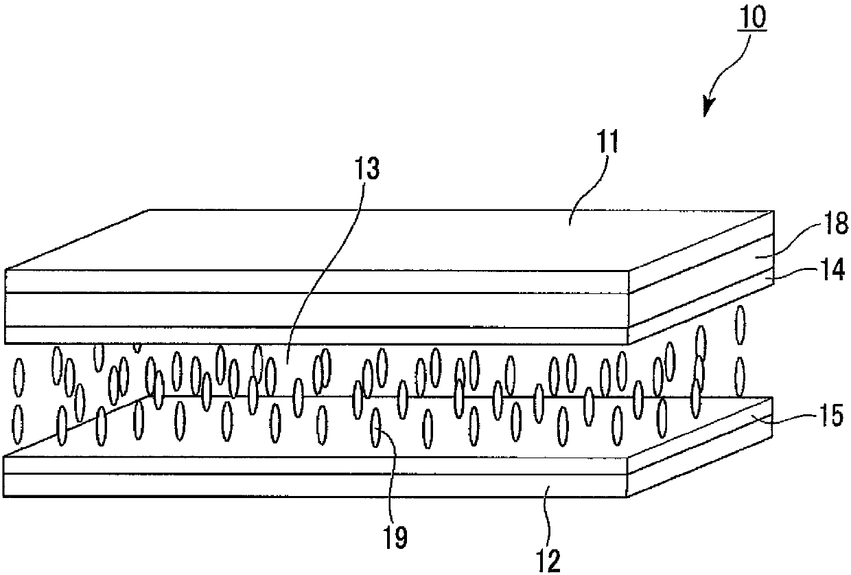
Although the MVA type liquid crystal display element has excellent viewing angle characteristics, the response speed of the liquid crystal molecules is different at the part separated from the protruding structure on the substrate. Due to the influence of molecules, there is a problem that the response speed as a whole is insufficient, and there is a problem that the transmittance decreases due to the protrusion structure.

Method used


Image

  • Liquid crystal display element and method for manufacturing same
  • Liquid crystal display element and method for manufacturing same
  • Liquid crystal display element and method for manufacturing same

Examples


Embodiment 1

[0308] Fabricate a first substrate (common electrode substrate) and a second substrate (pixel electrode substrate), the first substrate (common electrode substrate) has a transparent electrode layer and a color filter layer made of transparent common electrodes, the second substrate (Pixel electrode substrate) includes a pixel electrode layer having a transparent pixel electrode driven by an active element. Liquid crystal composition LC-1 containing a compound selected from the general formula (I) and a compound selected from the general formula (II) was prepared. The constituent compounds and the contained ratios are as follows.

[0309] [chem 38]

[0310]

[0311] For the liquid crystal composition LC-1 98.08wt%, add 1.5wt% of the polymerizable compound shown below,

[0312] [chem 39]

[0313]

[0314] Add 0.32wt% of the polymerizable compound shown below,

[0315] [chemical 40]

[0316]

[0317] And add 0.1wt% photopolymerization initiator Igacure651, and diss...

Embodiment 2

[0325] In the same experiment as in Example 1, 98.5 wt% of the liquid crystal composition LC-1 was added with 1.0 wt% of the polymerizable compound shown below,

[0326] [chem 41]

[0327]

[0328] Add 0.4wt% of the polymerizable compound shown below,

[0329] [chem 42]

[0330]

[0331] Furthermore, 0.1 wt % of photopolymerization initiator Igacure 651 was added and uniformly dissolved to prepare the polymerizable liquid crystal composition CLC-1a.

[0332]After the polymerizable liquid crystal composition CLC-1a was sandwiched between the common electrode substrate and the pixel electrode substrate not having an alignment film layer, the sealing material was cured to form a liquid crystal composition layer. At this time, a spacer having a thickness of 3.2 μm was used to make the thickness of the liquid crystal composition layer 3.2 μm. Ultraviolet rays are irradiated to the obtained liquid crystal display in a state where a voltage is applied to cure the polymerizab...

Embodiment 3

[0345] In the same experiment as in Example 1, the liquid crystal composition used was changed to liquid crystal composition LC-2 containing the compound selected from the general formula (I) and the compound selected from the general formula (II). The constituent compounds and the contained ratios are as follows.

[0346] [chem 43]

[0347]

[0348] For the liquid crystal composition LC-2 97.7wt%, add 1.8wt% of the polymerizable compound shown below,

[0349] [chem 44]

[0350]

[0351] Add 0.4wt% of the polymerizable compound shown below,

[0352] [chem 45]

[0353]

[0354] Furthermore, 0.1 wt % of photopolymerization initiator Igacure 651 was added and uniformly dissolved to prepare a polymerizable liquid crystal composition CLC-2.

[0355] After the polymerizable liquid crystal composition CLC-2 was sandwiched between the common electrode substrate and the pixel electrode substrate not having an alignment film layer, the sealing material was cured to form a l...


PUM


Abstract

Provided are: a liquid crystal display element in which ghosting and the occurrence of drop marks during manufacturing are suppressed without adversely affecting characteristics such as dielectric anisotropy, viscosity, nematic phase upper-limit temperature, and rotational viscosity ([gamma]1); and a method for manufacturing the liquid crystal display element. The present invention is characterized in that a liquid crystal layer containing a liquid crystal composition is sandwiched between a substrate having a shared electrode and color filters, and a substrate having a plurality of pixels andpixel electrodes for each of the pixels, by not having an alignment film on one or both of the substrates, and by having an alignment control layer formed from one or more species of trifunctional orgreater (meth)acrylate compounds and one or more species of bifunctional or monofunctional (meth)acrylate compounds. The present invention is applied as a liquid crystal display element for a liquidcrystal TV or the like.

Description

technical field [0001] The present invention relates to a liquid crystal display element useful as a constituent member of a liquid crystal TV or the like, and a method for manufacturing the same. Background technique [0002] Liquid crystal display components have developed from being used in clocks and calculators to various measuring equipment, automotive panels, word processors, electronic notepads, printers, computers, televisions, clocks, advertising display boards, etc. Typical liquid crystal display methods include TN (twisted nematic) type, STN (super twisted nematic) type, vertical alignment type (Vertical Alignment; VA) using TFT (thin film transistor), and IPS (in-plane switching) type etc. The liquid crystal composition used in these liquid crystal display elements is required to be stable against external factors such as moisture, air, heat, light, etc., and to display a liquid crystal phase in as wide a temperature range as possible around room temperature, t...

Claims


Application Information

Patent Timeline
Patent Type & Authority Applications(China)
IPC IPC(8): G02F1/1337C09K19/30C09K19/54G02F1/13G02F1/1368
CPCC09K2019/0448C09K2019/3004C09K2019/3009C09K2019/3027C09K2019/3016C09K2019/301C09K2019/123C09K19/542C09K19/3066C09K19/30C09K19/54G02F1/1337G02F1/1368G02F1/13G02F1/13775G02F1/133742G02F1/134345C09K19/3003C09K19/56G02F1/133707G02F1/1341G02F1/134336G02F1/137G02F2201/122G02F2201/123
Inventor 栗泽和树林正直
Owner DIC CORPORATION
Learn More