Indium electroplating composition containing 1,10-phenanthroline compound and method of electroplating indium
A composition and compound technology, applied in the direction of circuits, semiconductor devices, etc., can solve problems such as insufficient performance TIM, and achieve the effect of reducing damage
- Summary
- Abstract
- Description
- Claims
- Application Information
AI Technical Summary
Problems solved by technology
Method used
Image

Examples
example 1
[0053] Example 1 (comparison)
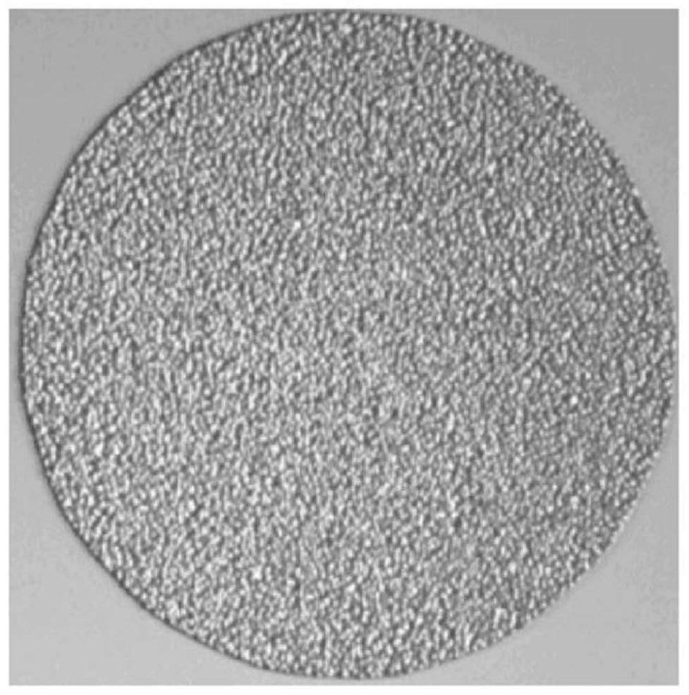
[0054] Photoresist patterned silicon wafers from Silicon Valley Microelectronics, Inc. using NIKAL from Dow Advanced Materials TM BP nickel plating bath plated with a layer of nickel, the silicon wafer had a plurality of via holes with a diameter of 75 μm and a copper seed layer at the base of each via hole. Nickel plating was performed at 55°C for 120 seconds at a cathodic current density of 1 ASD. A conventional rectifier supplies the current. The anode is a soluble nickel electrode. After plating, the silicon wafer was removed from the plating bath with a SHIPLEY BPR from Dow Advanced Materials TM The photo stripper strips the photoresist from the wafer and rinses with water. The nickel deposit appeared to be substantially smooth without any observable dendrites on the surface. Figure 1A for LEICA TM Optical image of one of the nickel-plated copper seed layers taken by an optical microscope.
[0055] The following aqueous indium elect...
example 2
[0061] The method described in Example 1 above was repeated except that the indium electroplating composition included the following components:
[0062] Table 2
[0063]
[0064]
[0065] A nickel plated silicon wafer is immersed in the indium electroplating composition and indium metal is plated on the nickel. Indium plating was performed at a current density of 4ASD for 30 seconds at 25°C. The pH of the composition is 2.1. The anode is an indium soluble electrode. After indium was electroplated on the nickel layer, the photoresist was stripped from the wafer and the indium morphology was observed. All indium deposits appeared uniform and smooth.
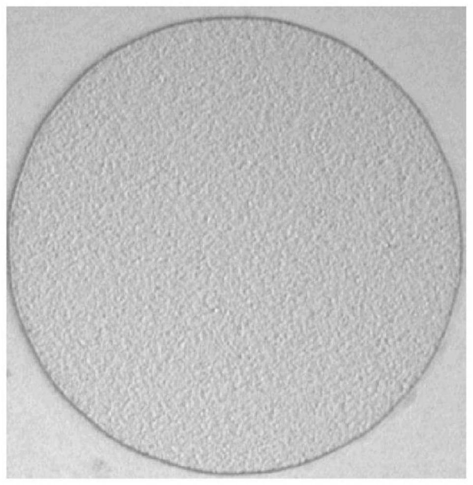
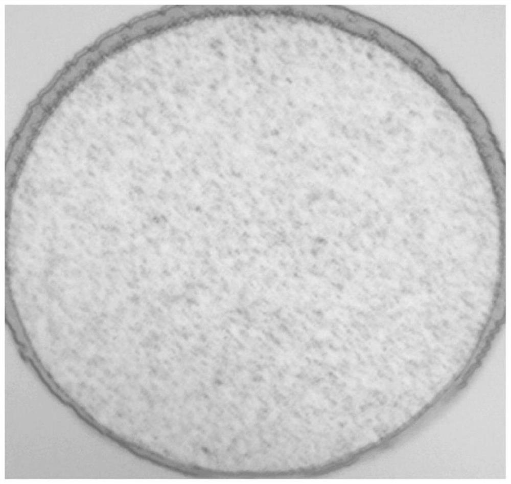
[0066] figure 2 is an optical microscope image of one of the indium metal deposits electroplated on a nickel layer. compared to Figure 1B Indium deposits, indium deposits appear smooth.
example 3
[0068] The method described in Example 2 above was repeated except that the indium electroplating composition included the following components:
[0069] table 3
[0070] components quantity Indium Sulfate 45g / L citric acid 96g / L Sodium Citrate Dihydrate 59g / L 1,10-phenanthroline 4ppm Sodium chloride 1
50g / L
[0071] 1 The molar ratio of chlorine: indium ion = 5:1
[0072] The pH of the indium composition is 2.4. A nickel plated silicon wafer is immersed in the indium electroplating composition and indium metal is plated on the nickel. Indium plating was performed at a current density of 4ASD for 30 seconds at 25°C. The anode is an indium soluble electrode. After indium was electroplated on the nickel layer, the photoresist was stripped from the wafer and the indium morphology was observed. All indium deposits appeared uniform and smooth.
[0073] image 3 is an optical microscope image of one of the indium metal d...
PUM
| Property | Measurement | Unit |
|---|---|---|
| diameter | aaaaa | aaaaa |
| molecular weight | aaaaa | aaaaa |
| aspect ratio | aaaaa | aaaaa |
Abstract
Description
Claims
Application Information
 - R&D
- Intellectual Property
- Life Sciences
- Materials
- Tech Scout
- Unparalleled Data Quality
- Higher Quality Content
- 60% Fewer Hallucinations
Browse by: Latest US Patents, China's latest patents, Technical Efficacy Thesaurus, Application Domain, Technology Topic, Popular Technical Reports.
© 2025 PatSnap. All rights reserved.Legal|Privacy policy|Modern Slavery Act Transparency Statement|Sitemap|About US| Contact US: help@patsnap.com