

Method for preparing silicon nanowire array based on metal assisted chemical etching technique
A silicon nanowire array and chemical etching technology, which is applied in the field of semiconductor nanomaterial preparation, can solve the problems of cumbersome process, high equipment requirements, and high production cost, and achieve the effect of solving cumbersome process
- Summary
- Abstract
- Description
- Claims
- Application Information
AI Technical Summary
Problems solved by technology
Method used
Image

Examples
Embodiment 1
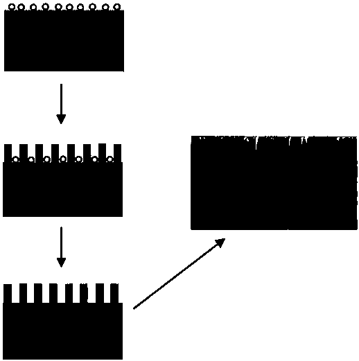
[0024] (1) Cleaning of silicon wafers: ultrasonically clean with acetone and absolute ethanol for 15-20 minutes in sequence, and then place the silicon wafers in H with a volume ratio of 1:1. 2 SO 4 and H 2 o 2 Boil them in the mixed solution for 3-5 minutes, then soak them in HF solution with a mass fraction of 3%-5% for 60-90s, and finally wash them with deionized water for 2-3 times, and then wash them with N 2 Blow dry; after each of the above steps is completed, it needs to be rinsed with deionized water 2 to 3 times;
[0025] (2) Deposition of Ag particles: Prepare the concentration ratio of HF:AgNO in a dark environment 3 =4.0 mol / L:0.005 mol / L equal-volume mixed solution, then ultrasonicated the plastic beaker containing the mixed solution for 5min, then placed the silicon wafer obtained in step (1) in the mixed solution, let it stand for 120s, and deposited Ag particles;
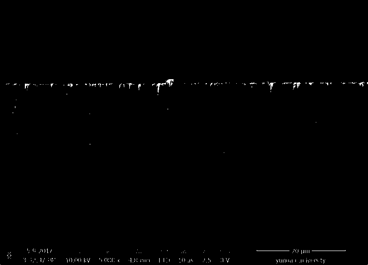
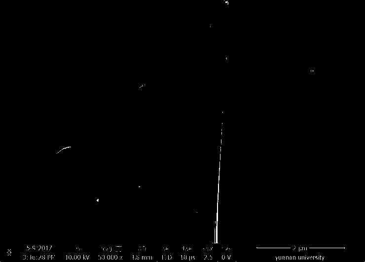
[0026] (3) Etching of nanowires: put the silicon wafer obtained in step (2) into a volume r...
Embodiment 2
[0031] (1) Cleaning of silicon wafers: ultrasonically clean with acetone and absolute ethanol for 15-20 minutes in sequence, and then place the silicon wafers in H with a volume ratio of 1:1. 2 SO 4 and H 2 o 2 Boil them in the mixed solution for 3-5 minutes, then soak them in HF solution with a mass fraction of 3%-5% for 60-90s, and finally wash them with deionized water for 2-3 times, and then wash them with N 2 Blow dry; after each of the above steps is completed, it needs to be rinsed with deionized water 2 to 3 times;
[0032] (2) Deposition of Ag particles: Prepare the concentration ratio of HF:AgNO in a dark environment 3 =5.0 mol / L: equal volume of 0.01 mol / L mixed solution, then sonicate the plastic beaker containing the mixed solution for 5min, then place the silicon wafer obtained in step (1) in the mixed solution, let it stand for 90s, and deposit Ag particles;
[0033] (3) Etching of nanowires: put the silicon wafer obtained in step (2) into a volume ratio of...
Embodiment 3
[0038] (1) Cleaning of silicon wafers: ultrasonically clean with acetone and absolute ethanol for 15-20 minutes in sequence, and then place the silicon wafers in H with a volume ratio of 1:1. 2 SO 4 and H 2 o 2 Boil them in the mixed solution for 3-5 minutes, then soak them in HF solution with a mass fraction of 3%-5% for 60-90s, and finally wash them with deionized water for 2-3 times, and then wash them with N 2 Blow dry; after each of the above steps is completed, it needs to be rinsed with deionized water 2 to 3 times;
[0039] (2) Deposition of Ag particles: Prepare the concentration ratio of HF:AgNO in a dark environment 3=5.0 mol / L: equal volume of 0.005 mol / L mixed solution, then sonicate the plastic beaker containing the mixed solution for 5 minutes, then place the silicon wafer obtained in step (1) in the mixed solution, let it stand for 110s, and deposit Ag particles;
[0040] (3) Etching of nanowires: put the silicon wafer obtained in step (2) into a volume ra...
PUM
| Property | Measurement | Unit |
|---|---|---|
| Length | aaaaa | aaaaa |
| Width | aaaaa | aaaaa |
| Length | aaaaa | aaaaa |
Abstract
Description
Claims
Application Information