
All-solid-state electric field reconfigurable magneto-optic device

A magneto-optical device, all-solid-state technology, applied in instruments, optics, nonlinear optics, etc., can solve the problems of difficult to achieve universality of magnetic regulation, incompatibility of semiconductor processes, non-volatile control, etc., and achieve poor process compatibility. , easy process compatibility, and the effect of improving device integration

Active Publication Date: 2018-02-09
UNIV OF ELECTRONIC SCI & TECH OF CHINA
View PDF3 Cites 0 Cited by
  • Summary
  • Abstract
  • Description
  • Claims
  • Application Information

AI Technical Summary

Problems solved by technology

[0014] In view of the above-mentioned problems or deficiencies, in order to simultaneously solve the problems of incompatibility between the existing technology and solid-state semiconductor technology, difficulty in controlling magnetism with electric field in a non-volatile manner, difficulty in realizing large-area magnetic regulation and universality, the present invention provides a An all-solid-state electric field reconfigurable magneto-optic device

Method used


Image

  • All-solid-state electric field reconfigurable magneto-optic device
  • All-solid-state electric field reconfigurable magneto-optic device
  • All-solid-state electric field reconfigurable magneto-optic device

Examples


Embodiment Construction

[0040] The present invention will be described in detail below in conjunction with embodiments and drawings.

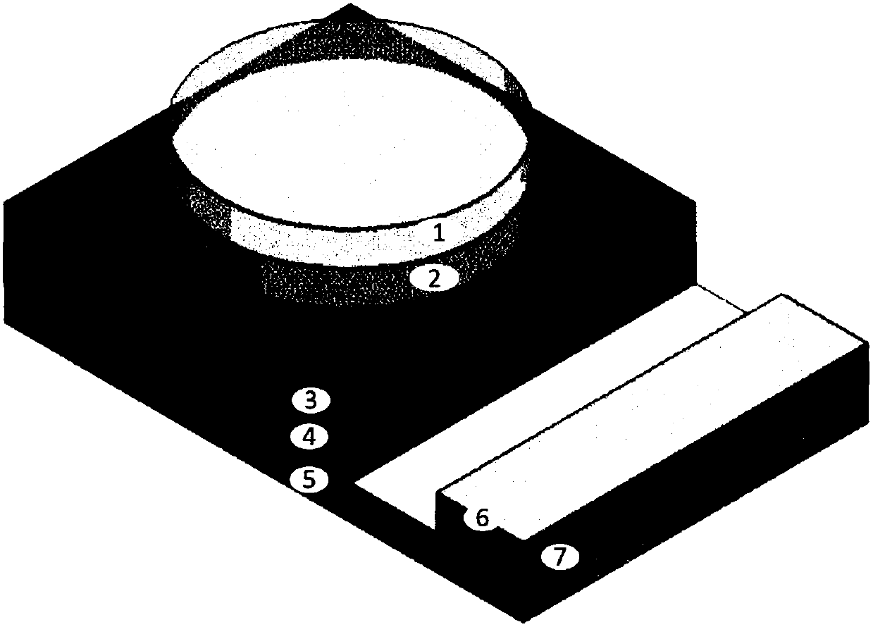
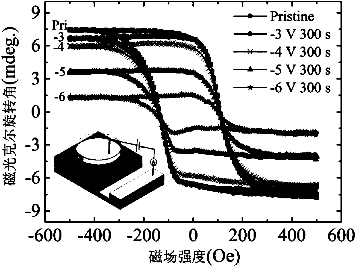
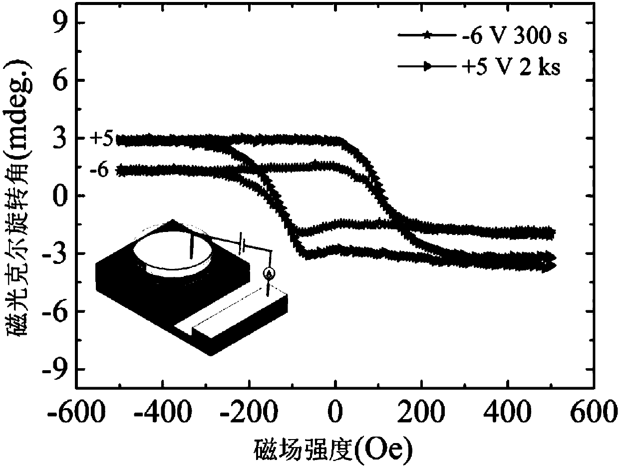
[0041] Device structure: a heavily doped p-type Si single crystal substrate is selected as the bottom electrode and plays a role in supporting the growth of the film, the thickness of the Si slice is 0.5mm; the yttrium iron garnet (chemical formula is Y 3 Fe 5 O 12 , The film thickness is 56.0nm) the film is used as the seed layer of lattice matching to grow the cerium-doped yttrium iron garnet film (chemical formula is CeY 2 Fe 5 O 12 , Film thickness 49.6nm), CeY 2 Fe 5 O 12 Is a magnetic medium layer; titanium oxide (chemical formula is TiO x , 0 x . The thickness of the gold top electrode is 6.4nm, and its diameter is 650μm (the diameter of the top electrode is too large to cause device breakdown; the diameter of the top electrode is related to the defect density in the bottom film and the breakdown field strength. The bottom film has low defect density and breakdown f...


PUM

PropertyMeasurementUnit
Thicknessaaaaaaaaaa

Abstract

The invention belongs to the technical field of magneto-optic devices, in particular to an all-solid-state electric field reconfigurable magneto-optic device. An all-solid-state structure is adopted,so that the structure is compatible with a semiconductor technology more easily; an electric field is utilized to manipulate the magneto-optic effect of magnetic film in a nonvolatile mode, and staticpower dissipation of the device is lowered; through the uniformity of ionic migration of an adjustable material layer, consistent manipulation of the magneto-optic effect within the range of severalhundred micron scales is achieved, and the problem that it is hard to scale down filament machine-made devices based on ionic conduction in equal proportion is solved; the adjustable material layer and a magnetic dielectric layer which are separated are adopted, and the purpose that the electric field manipulates the magneto-optic effect of a wide class of magnetic insulators or semiconductors isachieved. According to the all-solid-state electric field reconfigurable magneto-optic device, regarding one device, it is achieved that the structure is in an all solid state, the electric field manipulates the magneto-optic effect in a nonvolatile mode, the magneto-optic effect of the magnetic film is manipulated on a large scale and the magneto-optic effect of multiple magnetic insulators or semiconductors is manipulated in a generalization mode.

Description

Technical field [0001] The invention belongs to the technical field of magneto-optical devices, and relates to a magnetic oxide film material, in particular to an all-solid-state electric field reconfigurable magneto-optical device. Background technique [0002] At present, the magnetic control of most radio frequency and microwave magnetic devices and reconfigurable magneto-optical devices is realized by electric current driving electromagnets. Many shortcomings such as high power consumption, large volume, and high noise of electromagnets hinder the improvement of device performance. ([1]Liu M,Howe BM,Grazulis L,et al.Voltage-Impulse-Induced Non-VolatileFerroelastic Switching of Ferromagnetic Resonance for ReconfigurableMagnetoelectric Microwave Devices[J].Advanced Materials,2013,25(35):4886-92. [2]Huang D,Pintus P,Zhang C,et al.Dynamically reconfigurable integrated optical circulators[J].Optica, 2017,4(1):23-30.[3]Zhou Z.Voltage Control ofMagnetism[J].Ph .D thesis.2014.[4]Li...

Claims


Application Information

Patent Timeline
IPC IPC(8): G02F1/09
CPCG02F1/09G02F1/092
Inventor 毕磊朱银龙秦俊梁潇张燕王闯堂
Owner UNIV OF ELECTRONIC SCI & TECH OF CHINA
Learn More